preface
In the last introduction to the coding and decoding of hdb3, the coding rules of hdb3 are briefly introduced, and the simulation experiments are carried out with MATLAB. Interested friends can go and have a look. Encoding and decoding of HDB3 ① (realized by MATLAB) September 11, 2021 . After the simulation experiment, it will be implemented in FPGA. Through this study, we also have a further understanding of the relevant knowledge of FPGA. The following also introduces the design of relevant parts. The main references are: HDB3 encoder and decoder verilog code programming and Implementation This courseware gives a detailed design process, and the coding design mainly refers to the introduction of this courseware.
This article also introduces the implementation process of coding. The decoding process is described in the next article.
1, Steps to realize HDB3 coding
Sorting out the perfect logic is half the success. The coding of HDB3 to be realized should not be done too quickly. In the above courseware, the detailed process and corresponding code are given.
At the beginning of laioh hunger programming, I didn't quite understand what to replace V and B in hdb3 coding, and how to deal with the final positive and negative polarity? These problems are explained in the courseware.
Like MATLAB simulation, there are four symbols in the coding: 1, 0, B, V. Then use a two bit register to represent it respectively.
0: 00
1: 01
B: 10
V: 11
This is the beginning of "raw material" preparation. Let's start with modules.
There are three main processes:
Step 1: insert symbol V.
Step 2: insert symbol B.
The third step is to change the polarity as a whole. The values representing each symbol are unified into 0, + 1 and - 1.
Divided into modules, you can design one module by one.
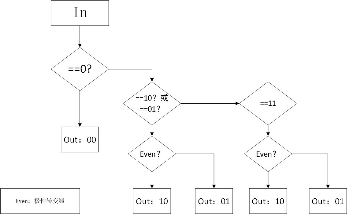
1. Insert V module
The first module is the plug-in V module. In this module, the input unipolar signal shall be transformed into a two bit signal, and V shall be inserted under the fixed format. So what is the fixed format? In the coding rules of HDB3, more than three zeros are not allowed to be continuous. If so, the fourth zero will be transformed into V, and the fourth zero is the position to insert v.
First, complete the logic block diagram.
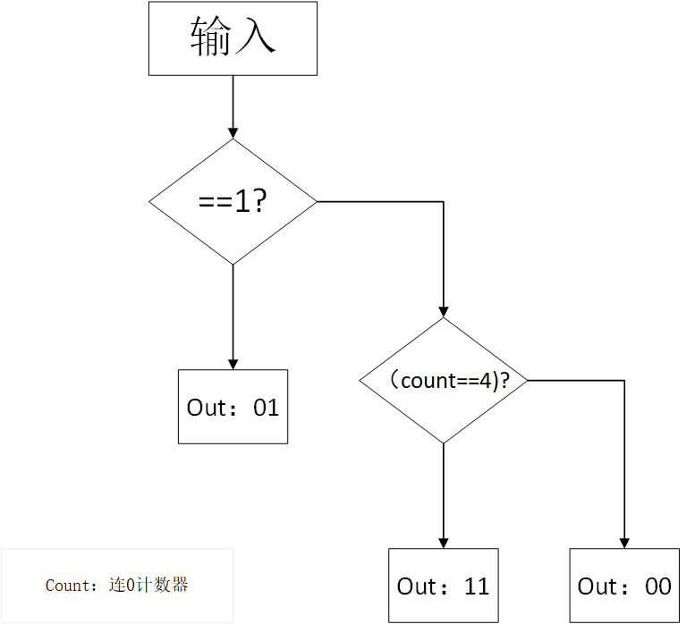
The overall logic is to judge, classify and re classify.
module add_v
(
	Clk,Rstn_,
	DataIn,DataOut
);

	input Clk;
	input Rstn_;

	input DataIn;

	output [1:0] DataOut;

	reg [1:0] DataOut;

	reg [1:0] count; //Even the "0" counter can have up to 4 zeros

	always @ (posedge Clk or negedge Rstn_)
		if (!Rstn_)
		begin
			count <= 2'd0;
			DataOut <= 2'b00;
		end
		else
		begin
			if (DataIn == 1'b1)  //If you receive 1
				begin
					count <= 2'd0;
					DataOut <= 2'b01;  //Don't consider polarity first
				end
			else
			begin
				count <= count + 1'b1;
				if (count == 2'd3) // Connect 0 to 4 outputs "V" 11
				begin
					count <= 2'd0;
					DataOut <= 2'b11;
				end
				else
					DataOut <= 2'b00; //Not up to 4 outputs connected to 0 00
			end
		end
endmodule
Take a brief look at the simulation results:
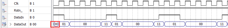
It can be seen that in the simulation result diagram, there is a small segment 00 in front of 01 at the start end, because the encoded value is 00 before the rising edge of the clock arrives. Thus, it can be concluded that an enable bit should be added when the hdb3 coding module is actually used. The order of use should be to give good data first, then quickly enable the module, and then encode, so as to ensure the overall coding quality.
2. Insert module B
Inserting module B can be said to be the core of the whole coding. It's still the same as smoothing out the logic. When will I insert B? When the number of 1s between two V is even, the first of the three zeros in front of the latter V needs to be transformed into B.
There are several important points:
The first point is to detect V and change the fourth value after V, so we need to design a four bit shift register. In this way, we can see both the front and the back.
The second point is how to deal with the problem of even numbers. How to judge whether the number of 1 is odd or even? The solution here is very awesome. We don't know how many 1s there will be between two V. there may be many or few, so it's impossible to count every 1. Here we use the feature of register overflow.
Define a one bit register with an odd number of 1, and the value of the register is 1. If there is an even number of 1, the value of the register is 0;
/**
 Time: September 9, 2021
 File name: add_B.v
 Project: hdb3 codec
 Top level module: hdb3.v
 Module name and Description: insert "B" during hdb3 coding
 Modification record: None
*/
module add_B
(
	Clk,Rstn_,
	DataIn_B,DataOut_B
);

	input Clk;
	input Rstn_;

	input [1:0] DataIn_B;

	output [1:0] DataOut_B;


	/****************V Counter design of and 1************************/

	reg count_1;  //Counter for '1'

	reg [1:0] count_V;  //Counter for "V"

	always @ (posedge Clk or negedge Rstn_)
		if (!Rstn_)
		begin
			count_1 <= 1'b0;
			count_V <= 1'b0;
		end
		else
		begin
			if(data[0] == 2'b11)  //The input is v. clear the counter of 1 and + 1 the counter of V
			begin
				count_1 <= 1'b0;
				count_V  = count_V + 1'b1;
			end
			else if(data[0] == 2'b01) //The input is the counter of 1 / / 1 plus 1
			begin
				count_1 <= count_1 + 1'b1;
				if(count_V  == 2'd2)//When this V becomes the rear V, change it back to the front v
					count_V <= 1'b1;
			end
			else			//The input is 0
			begin
				if(count_V  == 2'd2)//When this V becomes the rear V, change it back to the front v
					count_V <= 1'b1;
			end
		end


	/****************Four bit shift register************************/

	reg [1:0] data[3:0];
	reg [1:0] i;
	always @ (posedge Clk or negedge Rstn_)
		if (!Rstn_)
		begin
		//	for (i=0; i<3; i=i+1)
		//		data[i] <= 2'b0;
		end
		else
		begin
			data[3] <= data[2];
			data[2] <= data[1];
			data[1] <= data[0];
			data[0] <= DataIn_B;
		end


	/***************Design of data output port*************************/

	//count_ 1==0 && count_ V = = 1 means that the number of 1 is even
	//data[0]==2'b11 indicates that even numbers are counted between two V's
	assign DataOut_B = (count_1==0)&&(count_V==1)&&(data[0]==2'b11)? 2'b10:data[3];


endmodule
In the information given above, there is a small bug in the routine code in PPT, which has been corrected here. His bug is that if the source code starts at 110000... That is, there will be an even number of 1 at the beginning. Then he will also add B before the first V, which is unreasonable. The correction is given here.
Now let's analyze the working logic of each counter.
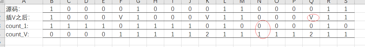
You can see that a B is inserted only when the number of 1 between two V is even.
Take a look at the simulation results:
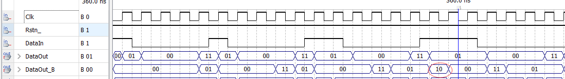
Due to the existence of four bit shift register, the output will lag four clocks. Also note that the first B should be 0, which is also a bug in the PPT.
3. Polarity
Through the sorting of the first two parts, the signal source code has been sorted into 00, 01, 10 and 11, that is, 0, 1, B and V. Here we start to sort out the polarity, and the output after sorting out the polarity should be 0, + 1, - 1. Here, 00 represents 0, 01 represents + 1 and 10 represents - 1;
The change rule of polarity is:
1.1 and B are regarded as a group, with positive and negative alternating changes. Generally, the polarity of the first 1 is negative.
2. The polarity of V is regarded as a group, with positive and negative alternating changes. The polarity of the first V is the same as that of the previous non-zero symbol.
Here, judge and sort out the data input from module B. Or simply draw a logic diagram.
Another function of the overall unity of polarity is to generate pulses. Of course, the two bits of output data can also be used as positive and negative pulses. Here, two ports are used to generate positive and negative pulses.
Overall Code:
module polar
(
	Clk,Rstn_,
	DataOut_B,PolarOut,
	BP,BN
);

	input Clk;
	input Rstn_;

	input [1:0] DataOut_B;

	output [1:0] PolarOut;

	//Design positive and negative pulses
	output BP;  // Positive pulse
	output BN;  // Negative pulse

	reg [1:0] PolarOut;

	reg BP;
	reg BN;

	/****************Polarity reversal************************/

	reg even = 0;

	always @ (posedge Clk or negedge Rstn_)
		if (!Rstn_)
		begin

		end
		else
		begin
			if( (DataOut_B == 2'b01) || (DataOut_B == 2'b10) ) //Enter 1 or B to flip
			begin
				if(even == 1) //Design the initial bit to - 1
					PolarOut <= 2'b01;
				else
					PolarOut <= 2'b10;
				even <= ~even; //Flip the identification bit
			end
			else if(DataOut_B == 2'b11) //The input is V
			begin
				if(even == 1)
					PolarOut <= 2'b10;
				else
					PolarOut <= 2'b01;
			end
			else  //Enter 00
				PolarOut <= 2'b00;
		end


	/****************Polarity reversal************************/

	always @ (posedge Clk or negedge Rstn_)
		if (!Rstn_)
		begin

		end
		else
		begin
			if(PolarOut == 2'b01) //The input is + 1
			begin
				BP <= 1'b1;
				BN <= 1'b0;
			end
			else if(PolarOut == 2'b10)  //The input is - 1
			begin
				BP <= 1'b0;
				BN <= 1'b1;
			end
			else
			begin
				BP <= 1'b0;
				BN <= 1'b0;
			end

		end
endmodule
The main point of attention is the polarity of 1 and V, which change alternately, but at the same time, the polarity of the first V is related to the polarity of the previous 1 (here 1 contains B). Here, a register even is used to control the overall polarity. Let's look at the simulation results.
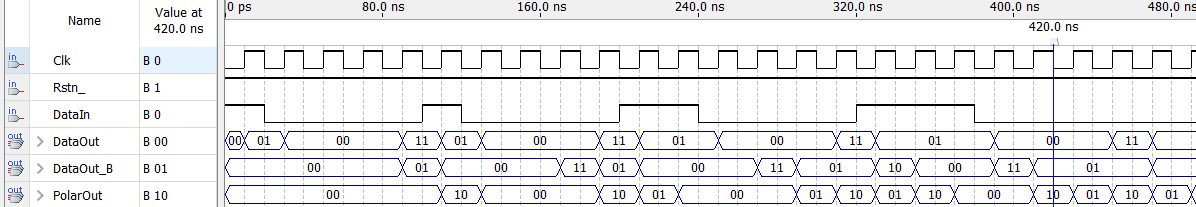
Compare with the results of your own manual calculation, you can get the corresponding results.
2, Summary
Through the coding of hdb3, I realized through this small subject that it is basically poor. In addition, I will not use the corresponding simulation tool, that is, ModelSim. I have always used the logic analyzer before. I have not used this kind of data simulation, which is the running time sequence. At this stage, I also summarized the most suitable development method for me, If you want to debug the program of timing class, you can use the logic analyzer if you have conditions for running timing. If you want to process the program of data coding, you still need to go to the simulation environment ModelSim. Accumulate. If you accumulate more, you will.