This is a summary I have made in my study. If there are copyright or knowledge errors, please contact me directly. Welcome to leave a message.
PS: Based on the principle of knowledge sharing, this blog can be reprinted, but please indicate the source!
Introduction:
Memory cell is almost indispensable in the design of a field bus.Whether it's a single port (SP), a simple dual port (SDP), or a true dual port (TDP), or whether it's implemented using BlockRAM or Distributed RAM, there are several ways to do this:
1), RTL code
It has strong controllability and measurability, but it may not get the best comprehensive results.
2),IP Core
Quick and flexible enough to achieve the desired overall result based on performance or resource requirements, but if needed
Change the implementation of Memory or IP version upgrade, you will need to call IP generation again
3),XPM_MEMORY
By contrast, XPM_MEMORY inherits the benefits of these approaches very well.
Key parameter description:
Refer to Xilinx for details UG974 Document
| Parameter Name | Default value | Explain |
| ADDR_WIDTH_A | 32 | Specifies the width, in units, of port A address port addra.Must be large enough to access the entire memory from port A, i.e. >=$clog2 (MEMORY_SIZE / WRITE_DATA_WIDTH_A). |
| AUTO_SLEEP_TIME | 0 | Number of clk[a|b] cycles of automatic sleep if functionality is available in the architecture * 0 - Disable Automatic Sleep * 3 - 15 - Number of automatic sleep delay cycles do not change the value instantiation provided in the template |
| BYTE_WRITE_WIDTH_A | 32 | Enable byte width writing on port A, specify the byte width in units * 8 - 8 - bit Byte Width Write when WRITE_DATA_WIDTH_A is valid when it is an integer multiple of 8 * 9 - 9 - Bit Byte Width Write, legal WRITE_DATA_WIDTH_A is an integer multiple of 9 or to enable word width writing on port A, specify with WRITE_DATA_WIDTH_A The same value. |
| CLOCKING_MODE | "common_clock" | * common_clock "- Universal clock;Provide a clock for port A and B using clka * independent_clock"- stand-alone clock;Clock Port A with clka and Port B with clkb |
| ECC_MODE | "no_ecc" | |
| MEMORY_OPTIMIZATION | "true" | "true" to enable optimizing unused memory or bits in memory structures. "false" to disable optimizing unused memory or bits in memory structures |
| MEMORY _PRIMITIVE | "auto" | Specify the memory primitive (resource type) to use ""auto"- Allow Vivado Synthesis to select" * distributed - distributed Memory * block - block Memory ""ultra"- hyper RAM memory" |
| MEMORY_SIZE | 2048 | Specifies the total memory array size in units.For example, for 2kx32RAM, enter 65536. * When ECC is enabled and set to "encode_When only', the memory size must be READ_DATA_WIDTH_Multiple of B * When ECC is enabled and set to "decode_When only', the memory size must be WRITE_DATA_WIDTH_Multiple of A |
| READ_DATA_WIDTH_B | 32 | Specifies the width, in units, of the port B read data output port doutb. * When ECC is enabled and set to "encode_When only', READ_DATA_WIDTH_B must be a multiple of 72 bits * When ECC is enabled and set to "decode_"Only" or "both_Encode_And_When decode, READ_DATA_WIDTH_B must be a multiple of 64 bits |
| READ_LATENCY_B | 2 | Specifies the number of register levels in the port B read data pipeline.Reading data output to port doutb requires this number of clkb cycles (when CLOCKING_MODE is "common_clock"is clka).To locate block memory, a value of 1 or more - 1 is required, causing only memory locks to be used;2 Causes the use of output registers.To locate distributed memory, a value of 0 or greater - 0 is required to represent the combined output.Values greater than 2 synthesize additional triggers that do not reschedule into memory primitives. |
| USE_EMBEDDED_CONSTRAINT | 0 | 1: Enable doutb_on clka and clkb of distributed RAM Set_between regsFalse_Path constraint addition |
| USE_MEM_INIT | 1 | |
| WAKEUP_TIME | "disable_sleep" | Specify "disable_sleep disables the dynamic energy saving option, specifying "use_sleep_pin"Enable Dynamic Energy Saving Options |
| WRITE_DATA_WIDTH_A | 32 | 64-bit multiplier when ECC is enabled and set to "decode_When only', WRITE_DATA_WIDTH_A must be a multiple of 72 bits |
| WRITE_MODE_B | "no_change" | "no _change", "read _first", "write _first" |
Instructions:
For illustration purposes, first exemplify the IP core settings:
As shown below, we will use asynchronous dual-port BRAM.
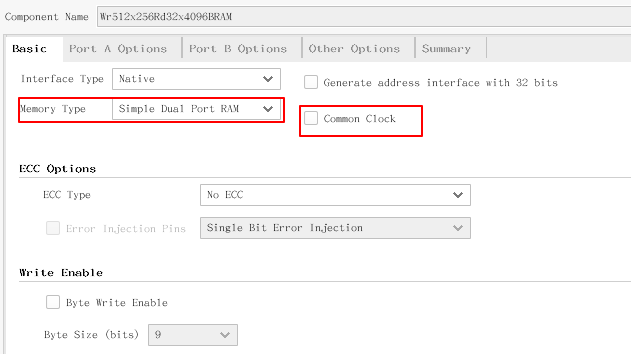
Write Bit Width 512 depth 2 ^ 8
Read Bit Width 32
The following are examples:
Wr512x256Rd32x4096BRAM u_RdBram(
    .clka   ( InDdrClk      ) , //: IN STD_LOGIC;
    .ena    ( 'b1           ) , //: IN STD_LOGIC;
    .wea    ( InRdBufEn     ) , //: IN STD_LOGIC_VECTOR(0 DOWNTO 0);
    .addra  ( InRdBufAddr   ) , //: IN STD_LOGIC_VECTOR(7 DOWNTO 0);
    .dina   ( InRdBufData   ) , //: IN STD_LOGIC_VECTOR(511 DOWNTO 0);
    .clkb   ( InRdBramClk   ) , //: IN STD_LOGIC;
    .enb    ( 'b1           ) , //: IN STD_LOGIC;
    .addrb  ( RdBramAddr    ) , //: IN STD_LOGIC_VECTOR(11 DOWNTO 0);
    .doutb  ( OutRdBramData )   //: OUT STD_LOGIC_VECTOR(31 DOWNTO 0)
  );
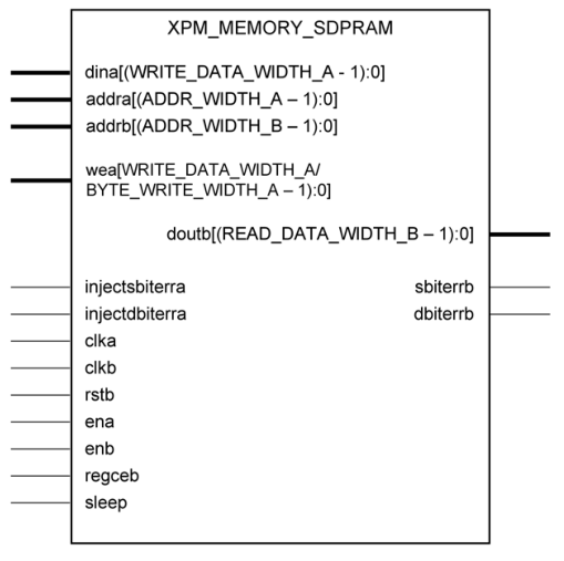
XPM_MEMORY reference code:
Where:
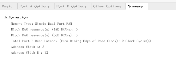
ADDR_WIDTH_A can refer to the IN STD_of IP Core LOGIC_VECTOR (7 DOWNTO 0);Set to 8;
ADDR_WIDTH_B refers to the IN STD_of IP Core LOGIC_VECTOR (11 DOWNTO 0);Set to 12;
CLOCKING_MODE set to asynchronous clock "independent_clock"
BYTE_WRITE_WIDTH_A and WRITE_DATA_WIDTH_A set to DDR_MIG_DW = 512
BYTE_WRITE_WIDTH_B set to 32
MEMORY_SIZE Set to: DDR_MIG_DW * 2 ^ 8
xpm_memory_sdpram #(
    .ADDR_WIDTH_A           ( 8                ) , // DECIMAL
    .ADDR_WIDTH_B           ( 12                        ) , // DECIMAL
    .AUTO_SLEEP_TIME        ( 0                         ) , // DECIMAL
    .BYTE_WRITE_WIDTH_A     ( DDR_MIG_DW                ) , // DECIMAL
    .CLOCKING_MODE          ( "independent_clock"       ) , // String
    .ECC_MODE               ( "no_ecc"                  ) , // String
    .MEMORY_INIT_FILE       ( "none"                    ) , // String
    .MEMORY_INIT_PARAM      ( "0"                       ) , // String
    .MEMORY_OPTIMIZATION    ( "true"                    ) , // String
    .MEMORY_PRIMITIVE       ( "block"                   ) , // String
    .MEMORY_SIZE            ( DDR_MIG_DW * 256          ) , // DECIMAL DDR_MIG_DW * 2^8
    .MESSAGE_CONTROL        ( 0                         ) , // DECIMAL
    .READ_DATA_WIDTH_B      ( 32                        ) , // DECIMAL
    .READ_LATENCY_B         ( 2                         ) , // DECIMAL
    .READ_RESET_VALUE_B     ( "0"                       ) , // String
    .USE_EMBEDDED_CONSTRAINT( 0                         ) , // DECIMAL
    .USE_MEM_INIT           ( 1                         ) , // DECIMAL
    .WAKEUP_TIME            ( "disable_sleep"           ) , // String
    .WRITE_DATA_WIDTH_A     ( DDR_MIG_DW                ) , // DECIMAL
    .WRITE_MODE_B           ( "no_change"               )   // String
) Wr512x256Rd32x4096(
    .dbiterrb               (                           ) , // 1-bit output
    .doutb                  ( OutRdBramData             ) , // READ_DATA_WIDTH_B-bit output
    .sbiterrb               (                           ) , // 1-bit output
    .addra                  ( InRdBufAddr               ) , // ADDR_WIDTH_A-bit input
    .addrb                  ( RdBramAddr                ) , // ADDR_WIDTH_B-bit input
    .clka                   ( InDdrClk                  ) , // 1-bit input
    .clkb                   ( InRdBramClk               ) , // 1-bit input
    .dina                   ( InRdBufData               ) , // WRITE_DATA_WIDTH_A-bit input
    .ena                    ( InRdBufEn                 ) , // 1-bit input
    .enb                    ( 1'b1                      ) , // 1-bit input
    .injectdbiterra         ( 1'b0                      ) , // 1-bit input
    .injectsbiterra         ( 1'b0                      ) , // 1-bit input
    .regceb                 ( 1'b1                      ) , // 1-bit input
    .rstb                   ( InDdrRst                  ) , // 1-bit input
    .sleep                  ( 1'b0                      ) , // 1-bit input
    .wea                    ( InRdBufEn                 ) // WRITE_DATA_WIDTH_A-bit input
);
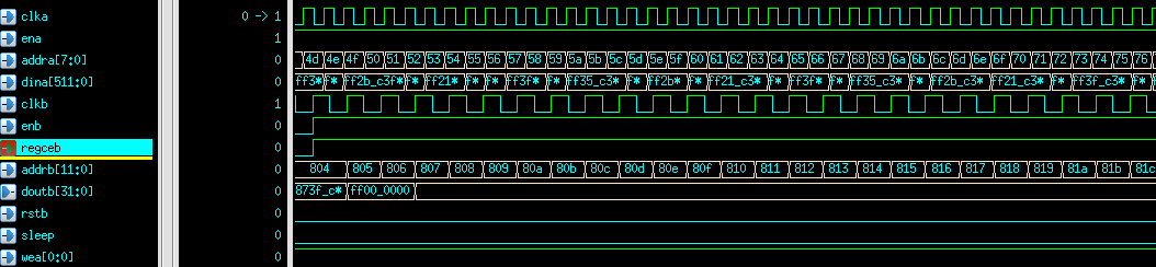
Note: It is recommended that enb be set to one, otherwise the last digit of the data will be read incorrectly!
The simulation results are as follows: