catalog
Experimental requirements
Step 1:
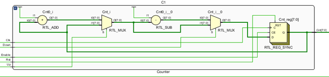
A add and subtract counter is designed, which is combined with binary to BCD decoder and alternating display control circuit in Experiment 1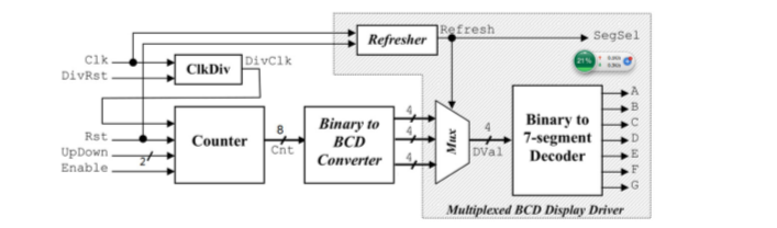
As shown in the figure:
Counter input: Clk,Up,Down,Rst,Enable
8bits output: Cnt7~Cnt0
Rst=1, the counter is cleared
Rst=0,Enable=1, then add one (Up=1) or subtract one (Down=1) to the upper or lower edge of each clock
Step 2
Change counter input to key control:
Basy3 circuit board (xc7a35tcpg336-1)
Press the Up key to count Up
The Down key represents the Down count
The middle key represents Enable and pause
Counter is initially idle
If the down key is captured, the count will start to decrease, and then the up key will be captured. Once the middle key is pressed, the counting process will be suspended; if the up key or down key is caught again, the counting will continue from the count before the pause
engineering structure
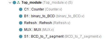
Core code
Counter module
The most important modules, the rest of which are based on the previous experiment:
module Counter(Clk,Up_set,Down_set,Rst_set,Enable_set,Cnt

    );
    input Clk;
    input Up_set;
    input Down_set;
    input Rst_set;
    input Enable_set;
    output reg [7:0] Cnt;
    reg [15:0] cnt_first;
    reg [15:0] cnt_second;
    reg CLK;
    reg [3:0]Chg;
    initial begin
        Cnt<=8'b00000000;
        Chg<=4'b0000;
        cnt_first<=16'b0;
        cnt_second<=16'b0;
    end
   always@(posedge Clk)begin
        if(cnt_first==16'd5000)
            cnt_first<=16'd0;
        else cnt_first<=cnt_first+1'b1;
   end
   always@(posedge Clk)begin
        if(cnt_first==16'd5000) cnt_second<=cnt_second+1'b1;
        if(cnt_second==16'd5000) begin
        cnt_second<=0;
        CLK=~CLK;
        end
        end
   always@(posedge Up_set or posedge Down_set or posedge Enable_set or posedge Rst_set)begin
       if(Rst_set==1) Chg<=4'b0000;
       else if(Up_set==1)  Chg<=4'b1001;
       else if(Down_set==1) Chg<=4'b1010;
       else if(Enable_set==1) Chg[3]<=~Chg[3];
       end
   always@(posedge CLK)begin
            case(Chg)
                4'b0000:Cnt<=8'b0;
                4'b1001:Cnt<=Cnt+1'b1;
                4'b1010:Cnt<=Cnt-1'b1;
            endcase
            end

endmodule
Among them:
always@(posedge Up_set or posedge Down_set or posedge Enable_set or posedge Rst_set)begin
       if(Rst_set==1) Chg<=4'b0000;
       else if(Up_set==1)  Chg<=4'b1001;
       else if(Down_set==1) Chg<=4'b1010;
       else if(Enable_set==1) Chg[3]<=~Chg[3];
       end
This part of code will report an error when implementing implementation:
[Designutils 20-970] Unrecognized or unsupported command 'set_property IOSTANDARD LVCMOS33 [get_ports {Enable]
set_property IOSTANDARD LVCMOS33 [get_ports {SegSel_n[3]}]
set_property IOSTANDARD LVCMOS33 [get_ports {SegSel_n[2]}]
set_property IOSTANDARD LVCMO ... (truncated) ' found in constraint file. ["C:/Users/18000/For_Ba_Counter/For_Ba_Counter.srcs/constrs_1/new/Constr.xdc":27]
Add to constraint file
set_property CLOCK_DEDICATED_ROUTE FALSE [get_nets Enable_IBUF]
set_property CLOCK_DEDICATED_ROUTE FALSE [get_nets Up_IBUF]
set_property CLOCK_DEDICATED_ROUTE FALSE [get_nets Down_IBUF]
Can solve the problem
Or change the code to:
always@(posedge CLK)begin
       if(Rst_set==1) Chg<=4'b0000;
       else if(Up_set==1)  Chg<=4'b1001;
       else if(Down_set==1) Chg<=4'b1010;
       else if(Enable_set==1) Chg[3]<=~Chg[3];
       end
This is a better way, in line with Verilog hardware programming principles
Top level module
module Top_module(Clk,Up,Down,SegSel_n,A,B,C,D,E,F,G,Enable,Rst

    );
    input Clk;
    input Up;
    input Down;
    input Enable;
    input Rst;
    output [3:0]SegSel_n;
    output A;
    output B;
    output C;
    output D;
    output E;
    output F;
    output G;
    wire [7:0] Cnt;
    wire [3:0]SegSel;
    Counter C1(.Clk(Clk),.Up_set(Up),.Down_set(Down),.Rst_set(Rst),.Enable_set(Enable),.Cnt(Cnt));
    wire [3:0]Hrs;
    wire [3:0]Tens;
    wire [3:0]Ones;
    binary_to_BCD B1(.SW(Cnt),.Hrs(Hrs),.Tens(Tens),.Ones(Ones));
    Refresh Refresh(.Clk(Clk),.Rst(1'b0),.SegSel(SegSel));
    wire [3:0]Dval;
    MUX MUX(.Refresh(SegSel),.Dval(Dval),.Hrs(Hrs),.Tens(Tens),.Ones(Ones));
    wire [6:0]L;
    BCD_to_7_segment S1(.X(Dval),.Lights(L));
    assign {A,B,C,D,E,F,G}=~L;
    assign SegSel_n=~SegSel;
endmodule
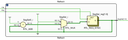
Refresh circuit
module Refresh(Clk,Rst,SegSel

    );
    input Clk,Rst;
    output reg [3:0]SegSel;
    initial begin
    SegSel=4'b0001;
    end
    reg [7:0] count_fst;
    reg[3:0]count_second;
    always@(posedge Clk)begin
        if(Rst==1) begin
            count_fst<=8'b00000000;
            SegSel<=4'b0000;
        end
        else begin
            if(count_fst==8'b11111111)
                begin
                count_fst<=4'b00000000;
                count_second<=count_second+1'b1;
                if(count_second==4'b1111)begin
                count_second<=4'b0000;
                case(SegSel)
                    4'b0000:SegSel<=4'b0001;
                    4'b0001:SegSel<=4'b0010;
                    4'b0010:SegSel<=4'b0100;
                    4'b0100:SegSel<=4'b1000;
                    4'b1000:SegSel<=4'b0001;
                    default:SegSel<=4'b0000;
                endcase
            end
            end
            else count_fst<=count_fst+8'b00000001;
        end
    end
endmodule
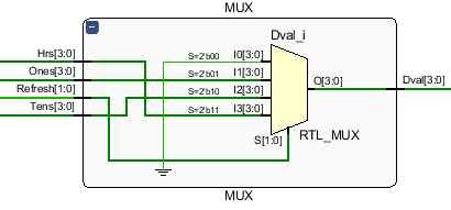
Multiplexer
module MUX(Refresh,Dval,Hrs,Tens,Ones

    );
    input [3:0] Refresh;
    input [3:0]Tens;
    input [3:0]Hrs;
    input [3:0]Ones;
    output reg [3:0]Dval;
    always@(*) begin
    case(Refresh)
        4'b0000:Dval=4'b0000;
        4'b0001:Dval=Ones;
        4'b0010:Dval=Tens;
        4'b0100:Dval=Hrs;
        default:Dval=4'b0000;
    endcase
    end

endmodule
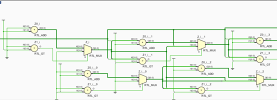
Binary to BCD decoder
module binary_to_BCD(SW,Hrs,Tens,Ones);
    input [7:0] SW;
    output [3:0]Hrs;
    output [3:0]Tens;
    output [3:0]Ones;
    reg [17:0] Z;
    always@(SW)begin
    Z=18'b0;
    Z[7:0]=SW;
    repeat(8)
    begin
    if(Z[11:8]>4)
        Z[11:8]=Z[11:8]+2'b11;
    if(Z[15:12]>4)
        Z[15:12]=Z[15:12]+2'b11;
    Z[17:1]=Z[16:0];
    end

    end
    assign Hrs=Z[17:16];
    assign Tens=Z[15:12];
    assign Ones=Z[11:8];

endmodule
BCD-to-7-Segment
module BCD_to_7_segment(X,Lights);
input [3:0] X;
output reg [6:0] Lights;
reg X3,X2,X1,X0;
reg A,B,C,D,E,F,G;
always @(X)begin
    {X3,X2,X1,X0}=X;
    case({X3,X2,X1,X0})
        4'd0:{A,B,C,D,E,F,G}=7'b1111110;
        4'd1:{A,B,C,D,E,F,G}=7'b0110000;
        4'd2:{A,B,C,D,E,F,G}=7'b1101101;
        4'd3:{A,B,C,D,E,F,G}=7'b1111001;
        4'd4:{A,B,C,D,E,F,G}=7'b0110011;
        4'd5:{A,B,C,D,E,F,G}=7'b1011011;
        4'd6:{A,B,C,D,E,F,G}=7'b1011111;
        4'd7:{A,B,C,D,E,F,G}=7'b1110000;
        4'd8:{A,B,C,D,E,F,G}=7'b1111111;
        4'd9:{A,B,C,D,E,F,G}=7'b1111011;
        default {A,B,C,D,E,F,G}=7'b0000000;
        endcase
        Lights={A,B,C,D,E,F,G};
        end
endmodule
Comprehensive results
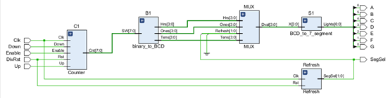
The structure is almost identical with the logic diagram given in the experiment
Refresh
Counter counting module
MUX module:
Seven bit decoder module:
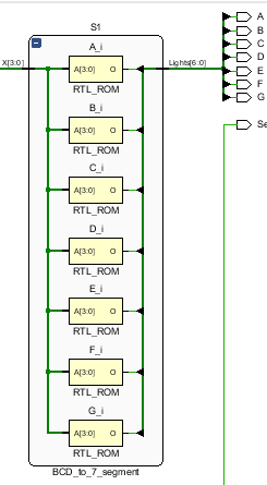
BCD decoder is an eight level iteration with the same structure as shown in the figure below
Pin constraint file
set_property PACKAGE_PIN W6 [get_ports B]
set_property PACKAGE_PIN U8 [get_ports C]
set_property PACKAGE_PIN V8 [get_ports D]
set_property PACKAGE_PIN U5 [get_ports E]
set_property PACKAGE_PIN U7 [get_ports G]
set_property PACKAGE_PIN T18 [get_ports Up]
set_property IOSTANDARD LVCMOS33 [get_ports A]
set_property IOSTANDARD LVCMOS33 [get_ports B]
set_property IOSTANDARD LVCMOS33 [get_ports C]
set_property IOSTANDARD LVCMOS33 [get_ports Clk]
set_property IOSTANDARD LVCMOS33 [get_ports D]
set_property IOSTANDARD LVCMOS33 [get_ports Down]
set_property IOSTANDARD LVCMOS33 [get_ports E]
set_property IOSTANDARD LVCMOS33 [get_ports F]
set_property IOSTANDARD LVCMOS33 [get_ports G]
set_property IOSTANDARD LVCMOS33 [get_ports Up]
set_property PACKAGE_PIN W5 [get_ports Clk]
set_property PACKAGE_PIN U17 [get_ports Down]
set_property PACKAGE_PIN W7 [get_ports A]
set_property PACKAGE_PIN V5 [get_ports F]
set_property IOSTANDARD LVCMOS33 [get_ports Enable]
set_property PACKAGE_PIN W4 [get_ports {SegSel_n[3]}]
set_property PACKAGE_PIN V4 [get_ports {SegSel_n[2]}]
set_property PACKAGE_PIN U4 [get_ports {SegSel_n[1]}]
set_property PACKAGE_PIN U18 [get_ports Enable]
set_property PACKAGE_PIN U2 [get_ports {SegSel_n[0]}]
set_property IOSTANDARD LVCMOS33 [get_ports {SegSel_n[3]}]
set_property IOSTANDARD LVCMOS33 [get_ports {SegSel_n[2]}]
set_property IOSTANDARD LVCMOS33 [get_ports {SegSel_n[1]}]
set_property IOSTANDARD LVCMOS33 [get_ports {SegSel_n[0]}]
set_property CLOCK_DEDICATED_ROUTE FALSE [get_nets Enable_IBUF]

set_property IOSTANDARD LVCMOS33 [get_ports Rst]
set_property PACKAGE_PIN W19 [get_ports Rst]