1: Preface
During this period, a friend and Wechat asked for help in debugging a PCIe card. The acquisition card uses xilinx xc7k410t as the controller and the upper computer is XP system. The original driving and testing software is based on xapp1052. As we all know, after Xilinx upgraded to Series 7, the original pcie ip core trn interface has been converted into axis interface, which saddens the friends who used xapp1052 before. It is not easy to use at once. How to transplant xapp1052 to K7 series of FPGA s seems to be very popular. In line with the principle of self-interest, the blogger turned over the remaining xapp1052 three or five years ago, slightly changed, and completed a version of BMD project that can be used in K7. In addition, the blogger provides a BMD project with FIFO as the user interface for friends who specialize in collecting cards.
II: Pre-preparation
1. The foundation of pcie should be established, especially the protocol part. Recommend a classic e-book, please read it patiently (Addison.Wesley.PCI.Express.System.Architecture.eBook-LiB.chm) download address: http://download.csdn.net/download/yuzeren48/7723815
2,pg054
3. Vivado 2018.2 Suite
4,Windriver
5,Visual studio 2010
3. Transplantation steps
1. Create an example project of K7 pcie ipcore in vivado.
2. Download xapp1052.pdf and xapp1052.zip on xilinx
3. Combine the codes of 1 and 2 projects and modify them slightly to form BMD project. 64-bit width (4x 2.5G) or 128-bit width (4x 5G) can be selected. The code level is as follows:
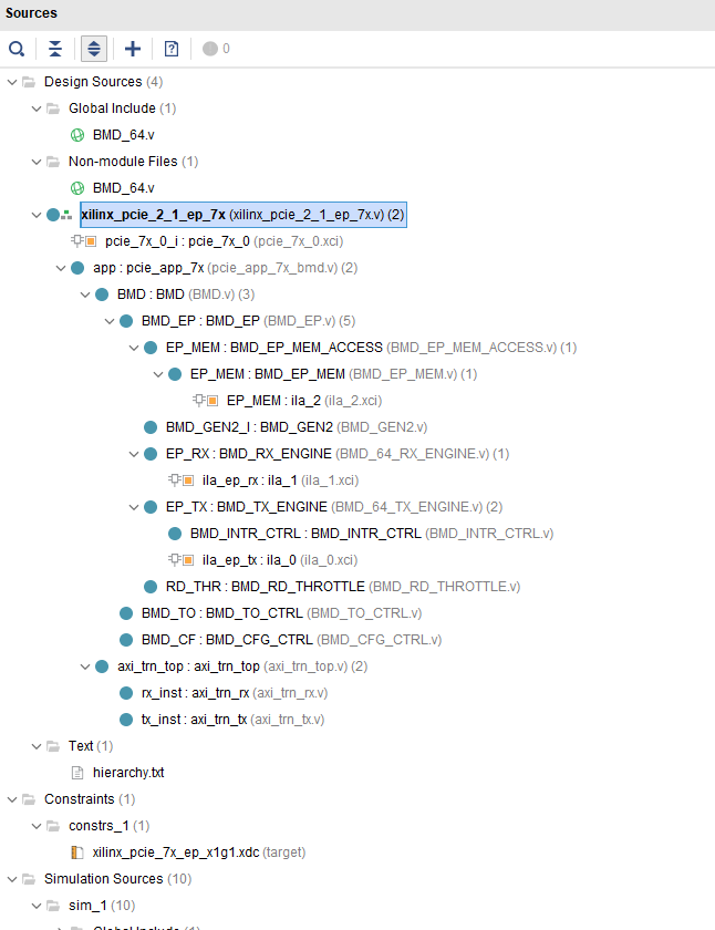
4. Key Code Analysis
1) All user status registers of BMD_EP_MEM-Control/Status Registers are in the module BMD_EP_MEM. All of our DMA transmission is to control these registers first, and then carry out the DMA transmission. After the transmission is completed, we get the transmission status by reading the value of the status register.
2) The function of EP_RX_ENGINE-Target module is implemented in EP_RX_ENGINE, which is responsible for receiving read and write TLP commands and submitting complete response of read and write memory. In EP_RX_ENGINE, Target receives 32-bit memory read request without data from PC and 32-bit memory write request with 1 DW word. The control state register is read and write through Target.
3) EP_RX_ENGINE-Rx engine Rx engine is not only responsible for receiving PC read-write memory requests, but also for completing the response (DMA transmission) of read-memory requests issued by the development board.
4) BMD_EP_MEM-Tx engine Tx engine not only receives and sends DMA data to PC, but also sends the complete response of read-write TLP package sent by PC.
5) All user status registers of BMD_EP_MEM-Control/Status Registers are in the module BMD_EP_MEM. All of our DMA transmission is to control these registers first, and then carry out the DMA transmission. After the transmission is completed, we get the transmission status by reading the value of the status register.
6) Interface bus interface, pcie-app_7x is the bus interface that includes all BMD.
AXI4-Stream to BMD interface axi_trn_rx module and axi_trn_tx implement the latest AXI4-Stream to BMD protocol. Some readers may doubt that the conversion protocol may affect the transmission efficiency, but there will be no sacrifice of efficiency, because here is the conversion of the protocol directly completed by the FPGA without any delay.
The author has made a very detailed comment on the key logic part of the code, the reader can buy according to the needs at the end of the article.
5. Software Code Analysis of PC
After installing windriver, we can find the corresponding driver files of BMD project in the WinDriver installation directory.
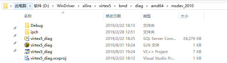
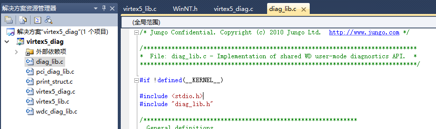
After opening with VS2010, the file directory is as follows. If you need to get the functional definition of functions in each C file, please purchase the corresponding information at the end of the article.
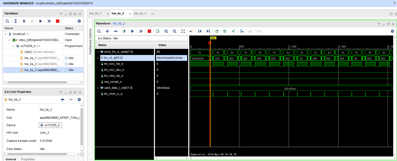
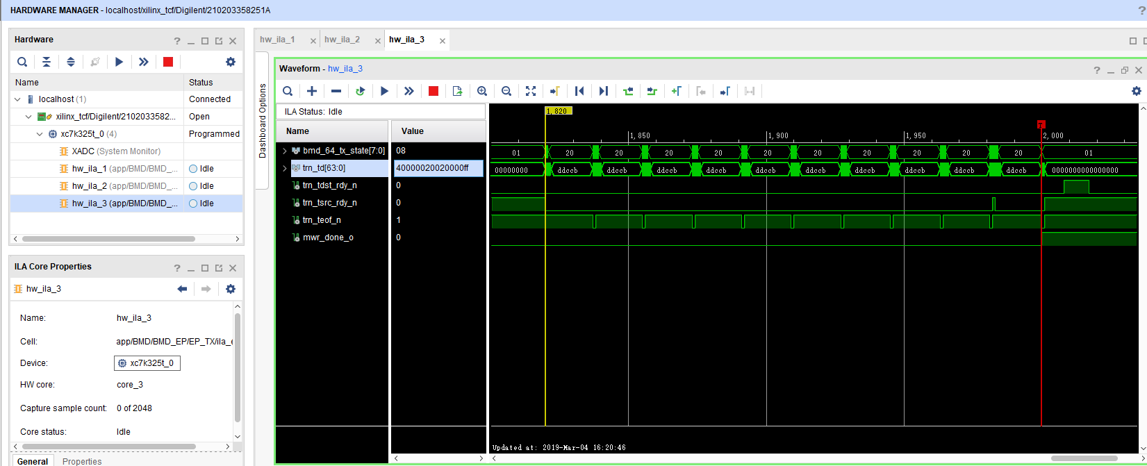
Running the test program and opening the VIVADO project grab package looks like the test code of V5, but we can find our own board by inputting VendorID and DeviceID.
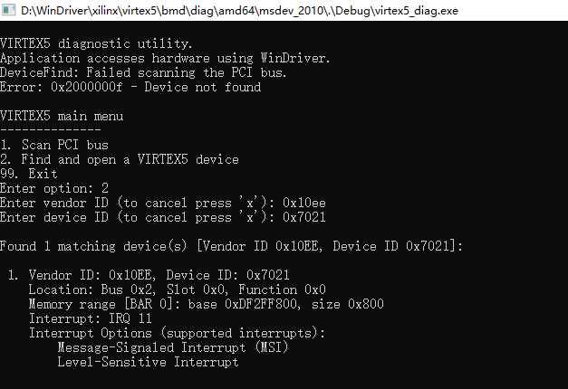
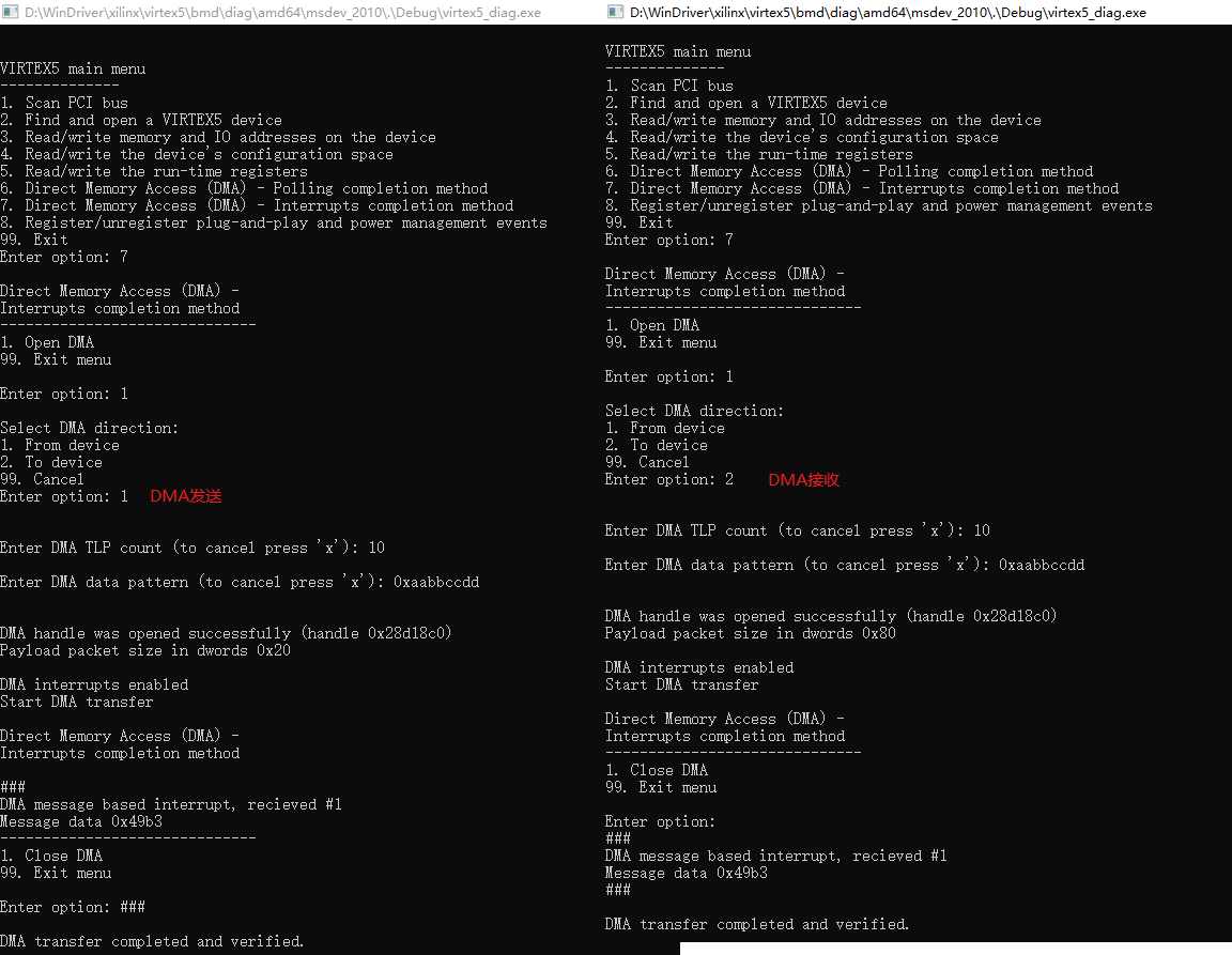
In the case of 4x GEN1(2.5G), continuous reading and writing tests show that the measured write bandwidth of PCIe is about 840MB/s and that of PCIe is about 761MB/s, which is almost full bandwidth.
4. Examples of Engineering
The above project is the transplantation test of xapp1052 on K7, but it is not practical for the friends who are engaged in engineering application. All the data read and written by DMA are fixed according to a patten register that our users configure themselves. If we want to transfer the data in FIFO to the system memory through xapp1052 DMA, we need to modify part of the source code. Here, the blogger provides you with a BMD project of FIFO interface for a fee.
The user interface is as follows:
module  pcie_app_7x#(
   parameter C_DATA_WIDTH = 64,            // RX/TX interface data width
   // Do not override parameters below this line
   parameter KEEP_WIDTH = C_DATA_WIDTH / 8  ,             // TKEEP width
   parameter REM_WIDTH  = (C_DATA_WIDTH == 128) ? 2 : 1 // trem/rrem width

)(

  input                         user_clk,
  input                         user_reset,
  input                         user_lnk_up,

  // Tx
  input  [5:0]                  tx_buf_av,
  input                         tx_cfg_req,
  input                         tx_err_drop,
  output                        tx_cfg_gnt,

  input                         s_axis_tx_tready,
  output  [C_DATA_WIDTH-1:0]    s_axis_tx_tdata,
  output  [KEEP_WIDTH-1:0]      s_axis_tx_tkeep,
  output  [3:0]                 s_axis_tx_tuser,
  output                        s_axis_tx_tlast,
  output                        s_axis_tx_tvalid,

  // Rx
  output                        rx_np_ok,
  output                        rx_np_req,
  input  [C_DATA_WIDTH-1:0]     m_axis_rx_tdata,
  input  [KEEP_WIDTH-1:0]       m_axis_rx_tkeep,
  input                         m_axis_rx_tlast,
  input                         m_axis_rx_tvalid,
  output                        m_axis_rx_tready,
  input    [21:0]               m_axis_rx_tuser,

  // Flow Control
  input  [11:0]                 fc_cpld,
  input  [7:0]                  fc_cplh,
  input  [11:0]                 fc_npd,
  input  [7:0]                  fc_nph,
  input  [11:0]                 fc_pd,
  input  [7:0]                  fc_ph,
  output [2:0]                  fc_sel,


  // CFG
  input  [31:0]                 cfg_do,
  input                         cfg_rd_wr_done,
  output [31:0]                 cfg_di,
  output [3:0]                  cfg_byte_en,
  output [9:0]                  cfg_dwaddr,
  output                        cfg_wr_en,
  output                        cfg_rd_en,

  output                        cfg_err_cor,
  output                        cfg_err_ur,
  output                        cfg_err_ecrc,
  output                        cfg_err_cpl_timeout,
  output                        cfg_err_cpl_abort,
  output                        cfg_err_cpl_unexpect,
  output                        cfg_err_posted,
  output                        cfg_err_locked,
  output [47:0]                 cfg_err_tlp_cpl_header,
  input                         cfg_err_cpl_rdy,
  output                        cfg_interrupt,
  input                         cfg_interrupt_rdy,
  output                        cfg_interrupt_assert,
  output [7:0]                  cfg_interrupt_di,
  input  [7:0]                  cfg_interrupt_do,
  input  [2:0]                  cfg_interrupt_mmenable,
  input                         cfg_interrupt_msienable,
  input                         cfg_interrupt_msixenable,
  input                         cfg_interrupt_msixfm,
  output                        cfg_turnoff_ok,
  input                         cfg_to_turnoff,
  output                        cfg_trn_pending,
  output                        cfg_pm_wake,
  input   [7:0]                 cfg_bus_number,
  input   [4:0]                 cfg_device_number,
  input   [2:0]                 cfg_function_number,
  input  [15:0]                 cfg_status,
  input  [15:0]                 cfg_command,
  input  [15:0]                 cfg_dstatus,
  input  [15:0]                 cfg_dcommand,
  input  [15:0]                 cfg_lstatus,
  input  [15:0]                 cfg_lcommand,
  input  [15:0]                 cfg_dcommand2,
  input   [2:0]                 cfg_pcie_link_state,

  output [1:0]                  pl_directed_link_change,
  input  [5:0]                  pl_ltssm_state,
  output [1:0]                  pl_directed_link_width,
  output                        pl_directed_link_speed,
  output                        pl_directed_link_auton,
  output                        pl_upstream_prefer_deemph,
  input  [1:0]                  pl_sel_link_width,
  input                         pl_sel_link_rate,
  input                         pl_link_gen2_capable,
  input                         pl_link_partner_gen2_supported,
  input  [2:0]                  pl_initial_link_width,
  input                         pl_link_upcfg_capable,
  input  [1:0]                  pl_lane_reversal_mode,
  input                         pl_received_hot_rst,

  output [63:0]                 cfg_dsn,
//user port
  output [63:0]                 RX_FIFO_DATA_o,
  output                        RX_FIFO_WR_o,
  input  [63:0]                 TX_FIFO_DATA_i,
  output                        TX_FIFO_RD_o,
  output [7:0]                  pcie_tap
)
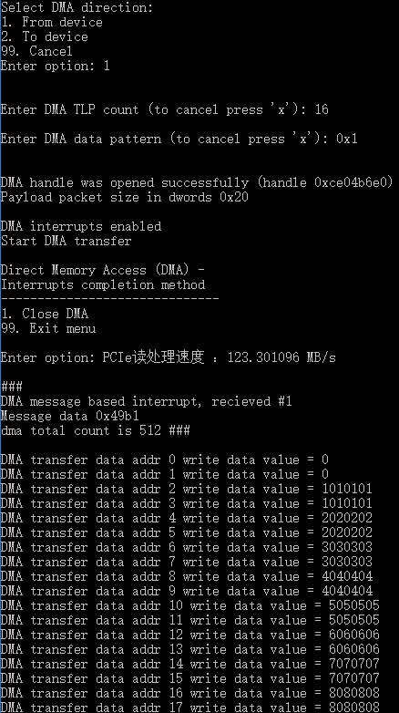
This interface can be directly connected to the CIE IP core interface of xilinx. User interface is very friendly to friends who make data acquisition cards. Here is an example of using XAPP1052 to collect data through FIFO. In order to verify the convenience of data, we count through a counter on the development board and send the value of the count to the upper computer. The test results are as follows:
In addition, we need to add that this project has no problem when DMA writes data, that is, when FPGA writes data to PC. But when the DMA reads data, that is, when the FPGA reads a large amount of data from the PC, the returned data will be out of order. This is a common problem of xapp1052, and it has no effect on friends who are collecting cards because they do not need to read data from the PC. If a friend needs to read and write correctly in the PCIe DMA project, you can contact me alone. I have a full set of PCIe DMA source code, which can be used in various series of FPGAs, but the price of the source code is not high.
Five, annex
1. xapp1052 K7 Transplantation Project with Hardware Code Notes and windows Driver Notes (200 yuan per copy)
2. xapp1052 K7 Transplantation Project (FIFO Interface), with Hardware Code Notes and windows Driver Instructions and Testing Programs (500 yuan per copy)
3. Supporting XILINX Series Multi-Channel PCIe DMA IP Core (Price Details)
If necessary, please send us a message (330853172)