SAC (Smart Analog Combo), i.e. intelligent simulation combination, the IP core does not take a long time to come out. At present, it is only used in two films: MSP430FR2353 and MSP430FR2355. First, let's look at the internal structure of SAC:
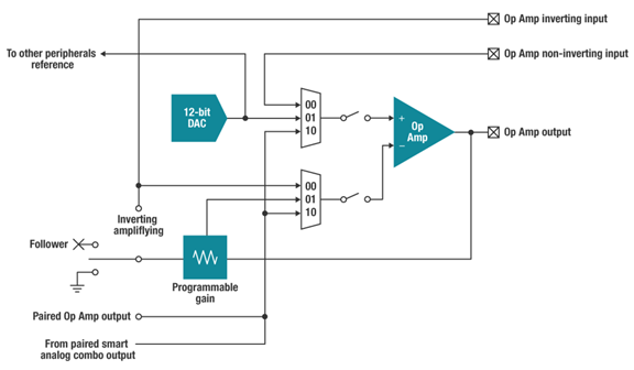
As can be seen from the above figure, the internal part is essentially an OPA amplifier. At the same time, there is a selection switch at the + and - input end of the operational amplifier, which can build different circuits according to the needs of customers. At the same time, a 12 bit DAC module is also integrated in the internal part, which is used to provide fixed voltage in some use environments and realize the purpose of voltage offset.
In view of the above internal structure, we make a detailed analysis:
For the + input, there are three channels to choose from:
00: pin in
01:12 bit DAC signal
10: The output of internal Amp, that is, the output of other SAC modules, is used for the combination of multi-level amps.
For - inputs, there are also three alternative channels:
00: pin access (the output of this Amp can also be selected to form a feedback circuit, or it can be directly grounded)
01: programmable gain
10: The output of internal Amp, that is, the output of other SAC modules, is used for the combination of multi-level amps.
So how to use it? What are the main aspects
In a word, as long as the circuit design of Amp is used, the resources of this module can be used. At the focus point, it is the detection of small current, such as blood glucose meter, blood oxygen meter, pulse detector, etc. in biotechnology. It can also be used to drive infrared or led with certain power.
Here are some common ways to connect:
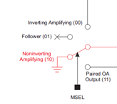
- General purpose mode
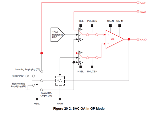
As shown in the general mode above, the positive and negative terminals of OA select external pins as input, and the output terminal does not feed back, so it can be used as an OA directly, and users can build their own peripheral circuits.
- Buffer mode
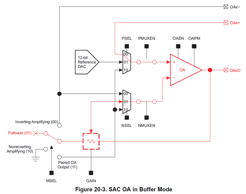
The above circuit topology is the connection mode of voltage follower and voltage buffer (there are some differences between follower and buffer, not to elaborate). It can be used when users require high input impedance and low output impedance.
- Reversing mode
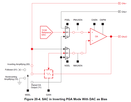
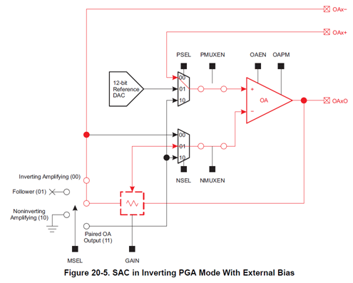
Reverse mode, as shown above, this kind of circuit structure should be the most used circuit by the user. The negative terminal is the input, and the positive terminal can provide a required bias voltage. The specific formula is not detailed, and the data is much simpler.
For the bias voltage provided by the positive terminal, there are two ways: internal 12 bitDAC and direct external voltage. This is the two structures shown above.
- Noninverting mode
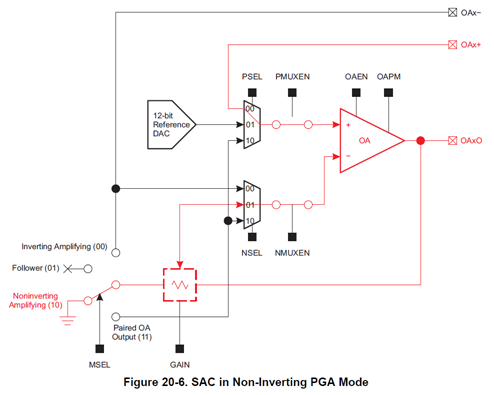
The topology of this circuit is in-phase mode. The input is from the positive side, and the negative side and the output are connected by adjustable gain to form a feedback circuit.
SAC is essentially an operational amplifier structure. At the same time, it is equipped with multiple selection switches at the input and output terminals, so that users can avoid external resistance, capacitance and other circuits in the use process, save board space, and also accelerate user design. At the same time, the internal SAC modules can be cascaded for multi-level amplification, which is more convenient to use. So how to set up the internal circuit structure? Operation register, of course! The following details the relevant register settings and gives the reference program.
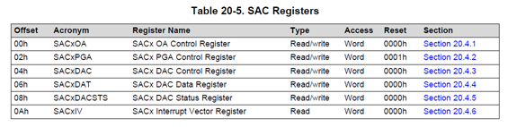
First, take a look at the contents of registers as a whole. The SAC module includes six registers, as follows:
- SACxOA
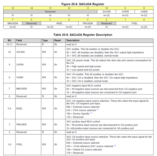
Sacen: enable bit of SAC module, enable all SAC modules when 1, output bit high resistance state when disabled.
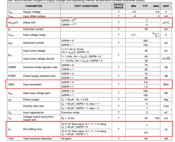
Oapm: the mode selection of OA, that is, it can be high-speed or low-speed. Of course, high-speed or low-speed will affect power consumption, bandwidth, speed, etc. for specific parameters, please refer to the chip's datasheet, as shown in the figure below for FR2355 data.
OAEN: internal OA enable, this bit is used to control the enable of OA module inside SAC.
NMUXEN: this bit controls the enabling of the negative input of OA. From the internal structure diagram, we can see that there are two levels before the negative input of OA: MUX in the first level, i.e. selecting the input source, and MUX in the second season. That is to say, even if the input source of MUX is selected, this must be enabled, otherwise MUX and the negative input of OA will be disconnected.
NSEL: negative input selection bit.
PMUXEN: this bit is similar to NMUXEN at the negative end, which controls the connection or disconnection of MUX at the positive end and OA.
PSEL: positive input selection bit.
- SACxPGA
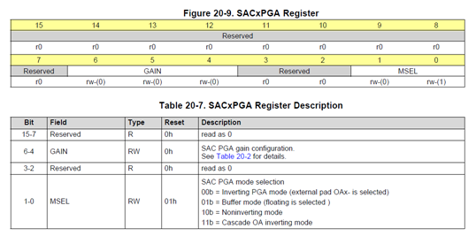
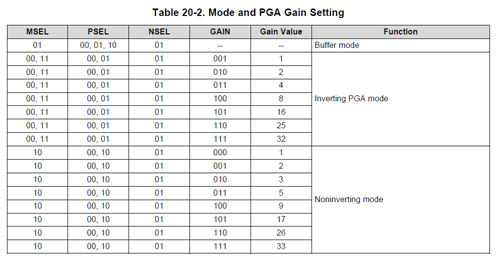
Gain: OA gain selection, that is, the setting bit of adjustable gain in the figure above, has three bits. With NSEL PSEL MSEL, gain selection in multiple modes can be realized.
MSEL: the selection of PGA mode controls the internal circuit structure as shown in the figure below:
To sum up, it can be found that circuit topology, i.e. gain and other parameters are related to MSEL PSEL NSEL GAIN. How to set these parameters? The following figure gives some examples of parameters. During the use, you can set the register according to the following data.
- SACxDAC
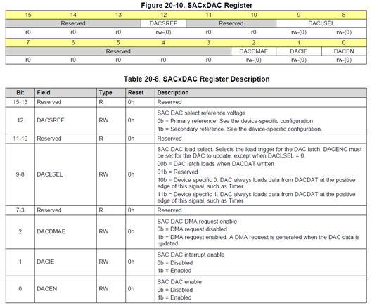
The SACxDAC register is obviously used to control the 12 bit DAC module inside the SAC. What is the circuit structure of the internal DAC module like?
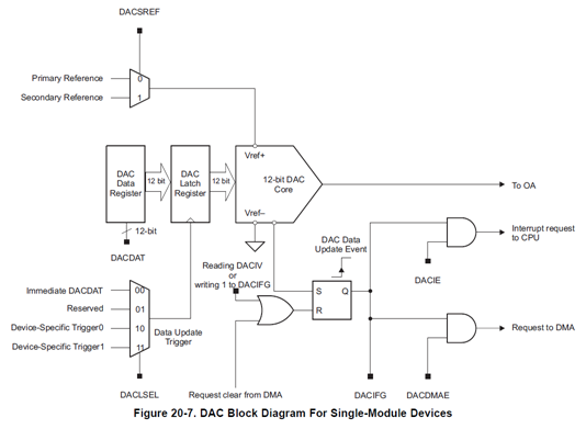
Then we can easily understand the meaning of each bit in this register by looking at the internal structure diagram of DAC.
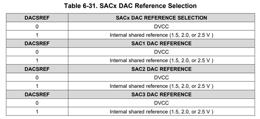
DACSREF: this bit determines the reference voltage of DAC. There are two options: primary and secondary. The reference source of each item can be seen in the chip's datasheet, as shown in the figure below is the information of FR2355.
DACLSEL: as can be seen from the above structure, this bit determines whether the set DAC value enters the DAC CORE. When the set data enters the DAC CORE, it will drive the corresponding voltage output, that is to say, this bit determines the frequency of voltage change of the DAC CORE, which can be real-time or pulse controlled.
Dacmae: DMA request enable in DAC. When DAC data is updated, if this bit is enabled, there will be a DMA request.
Dacie: the enable signal of DAC interrupt. When DAC data is updated, an interrupt signal can be generated to CPU.
Dacen: DAC enable bit.
- SACxDAT
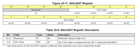
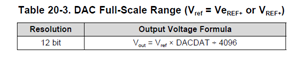
This register is used to set the DAC voltage value. What is the DAC output voltage value? Calculate according to the following formula:
- SACxDACSTS
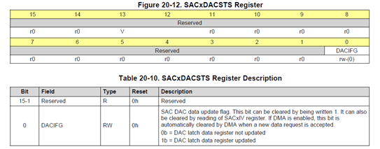
This register is the status flag register of DAC. At present, only 0 bit is used for dacfg, and others are reserved.
Dacfg is the flag bit of DAC data update.
- SACxIV
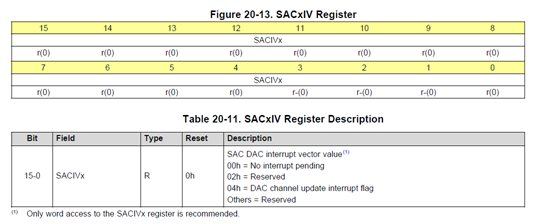
DAC interrupt vector register, read-only register, is related to the interrupt generated by the internal data update of DAC. When an interrupt is generated, the program at the interrupt vector will be triggered, and then the user's interrupt service program can be executed.
Well, after describing all registers of SAC, several routines are provided for your reference (MSP430FR2355):
- General Purpose Mode:
#include <msp430.h>

int main(void)
{
  WDTCTL = WDTPW + WDTHOLD;                 // Stop watch dog timer

  P1SEL0 |= BIT1 + BIT2 + BIT3;             // Select P1.1 P1.2 P1.3 OA function
  P1SEL1 |= BIT1 + BIT2 + BIT3;             // Select P1.1 P1.2 P1.3 OA function

  SAC0OA |= NMUXEN + PMUXEN;                // Enable negative and positive input
  SAC0OA |= OAPM;                           // Select low speed and low power mode
  SAC0OA |= SACEN + OAEN;                   // Enable SAC and OA

  __bis_SR_register(LPM3_bits);             // Enter LPM3
}
- Buffer Mode:
#include <msp430.h>

int main(void)
{
  WDTCTL = WDTPW + WDTHOLD;                 // Stop watch dog timer

  P1SEL0 |= BIT1 + BIT3;                    // Select P1.1 P1.3 as external OA function
  P1SEL1 |= BIT1 + BIT3;                    // Select P1.1 P1.3 as external OA function

  SAC0OA |= NMUXEN + PMUXEN + NSEL_1 + OAPM;// Enable negative and positive input
                                            // Select PGA source as OA negative input
                                            // Select low speed and low power mode
  SAC0PGA |= MSEL_1;                        // Set as Unity-Gain Buffer Mode
  SAC0OA |= SACEN + OAEN;                   // Enable SAC and OA

  __bis_SR_register(LPM3_bits);             // Enter LPM3
}- Inverting Mode:
#include <msp430.h>

int main(void)
{
  WDTCTL = WDTPW + WDTHOLD;                 // Stop watch dog timer

  // Disable the GPIO power-on default high-impedance mode
  // to activate previously configured port settings
  PM5CTL0 &= ~LOCKLPM5;

  // Configure reference module
  PMMCTL0_H = PMMPW_H;                    // Unlock the PMM registers
  PMMCTL2 = INTREFEN | REFVSEL_0;         // Enable internal 1.5V reference
  while(!(PMMCTL2 & REFGENRDY));          // Poll till internal reference settles

  P1SEL0 |= BIT1 | BIT2 | BIT3;             // Select P1.1 P1.2 P1.3 OA function
  P1SEL1 |= BIT1 | BIT2 | BIT3;             // Select P1.1 P1.2 P1.3 OA function

  SAC0DAC = DACSREF_1;                       // Select 1.5V int Vref as DAC reference
  SAC0DAT = 0x0FFF;                         // Set SAC DAC data to 1.5V
  SAC0DAC |= DACEN;                         // Enable DAC
  SAC0OA = NMUXEN + PMUXEN + PSEL_1 + NSEL_1;//Select positive and negative pin input
  SAC0OA |= OAPM;                           // Select low speed and low power mode
  SAC0PGA = GAIN2 + MSEL_0;                 // Set inverting PGA mode with Gain=8
  SAC0OA |= SACEN + OAEN;                   // Enable SAC and OA

  __bis_SR_register(LPM3_bits);             // Enter LPM3
}- Non-inverting Mode:
#include <msp430.h>

int main(void)
{
  WDTCTL = WDTPW + WDTHOLD;                 // Stop watch dog timer

  P1SEL0 |= BIT1 + BIT2 + BIT3;             // Select P1.1 P1.2 P1.3 OA function
  P1SEL1 |= BIT1 + BIT2 + BIT3;             // Select P1.1 P1.2 P1.3 OA function

  SAC0OA = NMUXEN + PMUXEN + PSEL_0 + NSEL_1;//Select positive and negative pin input
  SAC0OA |= OAPM;                           // Select low speed and low power mode
  SAC0PGA = GAIN0 + GAIN2 + MSEL_2;         // Set Non-inverting PGA mode with Gain=17
  SAC0OA |= SACEN + OAEN;                   // Enable SAC and OA

  __bis_SR_register(LPM3_bits);             // Enter LPM3
}
- DAC Buffer Mode: Output DAC data and use SAC as DAC
#include <msp430.h>

unsigned int DAC_data=0;

int main(void)
{
  WDTCTL = WDTPW + WDTHOLD;                 // Stop watch dog timer

  P1SEL0 |= BIT1;                           // Select P1.1 as OA0O function
  P1SEL1 |= BIT1;                           // OA is used as buffer for DAC

  PM5CTL0 &= ~LOCKLPM5;          // Disable the GPIO power-on default high-impedance mode
                                 // to activate previously configured port settings

  // Configure reference module
  PMMCTL0_H = PMMPW_H;                      // Unlock the PMM registers
  PMMCTL2 = INTREFEN | REFVSEL_2;           // Enable internal 2.5V reference
  while(!(PMMCTL2 & REFGENRDY));            // Poll till internal reference settles

  SAC0DAC = DACSREF_1 + DACLSEL_2 + DACIE;  // Select int Vref as DAC reference
  SAC0DAT = DAC_data;                       // Initial DAC data
  SAC0DAC |= DACEN;                         // Enable DAC
  SAC0OA = NMUXEN + PMUXEN + PSEL_1 + NSEL_1;//Select positive and negative pin input
  SAC0OA |= OAPM;                            // Select low speed and low power mode
  SAC0PGA = MSEL_1;                          // Set OA as buffer mode
  SAC0OA |= SACEN + OAEN;                    // Enable SAC and OA

  // Use TB2.1 as DAC hardware trigger
  TB2CCR0 = 100-1;                           // PWM Period/2
  TB2CCTL1 = OUTMOD_6;                       // TBCCR1 toggle/set
  TB2CCR1 = 50;                              // TBCCR1 PWM duty cycle
  TB2CTL = TBSSEL__SMCLK | MC_1 | TBCLR;     // SMCLK, up mode, clear TBR

  __bis_SR_register(LPM3_bits + GIE);        // Enter LPM3, Enable Interrupt
}

#if defined(__TI_COMPILER_VERSION__) || defined(__IAR_SYSTEMS_ICC__)
#pragma vector = SAC0_SAC2_VECTOR
__interrupt void SAC0_ISR(void)
#elif defined(__GNUC__)
void __attribute__ ((interrupt(SAC0_SAC2_VECTOR))) SAC0_ISR (void)
#else
#error Compiler not supported!
#endif
{
  switch(__even_in_range(SAC0IV,SACIV_4))
  {
    case SACIV_0: break;
    case SACIV_2: break;
    case SACIV_4:
        DAC_data++;
        DAC_data &= 0xFFF;
        SAC0DAT = DAC_data;                 // DAC12 output positive ramp
        break;
    default: break;
  }
}- SAC0 + SAC2 cascade mode:
#include <msp430.h>

unsigned int adcResult;

int main(void)
{
  WDTCTL = WDTPW + WDTHOLD;                 // Stop watchdog timer

  P1DIR |= BIT0;                            // Select P1.0 as output
  P1OUT &= ~BIT0;                           // Set P1.0 output low

  PM5CTL0 &= ~LOCKLPM5;       // Disable the GPIO power-on default high-impedance mode
                              // to activate previously configured port settings

  //Select P1.1 P1.2 P1.3 as SAC0 function
  //Select P3.1 P3.2 P3.3 as SAC2 function
  P1SEL0 |= BIT1 + BIT2 + BIT3;
  P1SEL1 |= BIT1 + BIT2 + BIT3;
  P3SEL0 |= BIT1 + BIT2 + BIT3;
  P3SEL1 |= BIT1 + BIT2 + BIT3;

  SAC2OA = NMUXEN + PMUXEN + PSEL_0 + NSEL_1;//Select positive and negative pin input
  SAC2OA |= OAPM;                           // Select low speed and low power mode
  SAC2PGA = GAIN1 + MSEL_2;                 // Set Non-inverting PGA mode with Gain=3
  SAC2OA |= SACEN + OAEN;                   // Enable SAC2 and OA
  SAC0OA = NMUXEN + PMUXEN + PSEL_2 + NSEL_1;//Select Pair OA source
  SAC0OA |= OAPM;                           // Select low speed and low power mode
  SAC0PGA = GAIN0 + GAIN1 + MSEL_2;         // Set Non-inverting PGA mode with Gain=5
  SAC0OA |= SACEN + OAEN;                   // Enable SAC0 and OA

  // Configure ADC12
  ADCCTL0 &= ~ADCENC;                       // Disable ADC
  ADCCTL0 = ADCSHT_2 | ADCON;               // ADCON, S&H=16 ADC clks
  ADCCTL1 = ADCSHP;                         // ADCCLK = MODOSC; sampling timer
  ADCCTL2 = ADCRES_2;                       // 12-bit conversion results
  ADCIE = ADCIE0;                           // Enable ADC conv complete interrupt
  ADCMCTL0 = ADCINCH_1 | ADCSREF_0;         // A1 ADC input select = OA0 output
                                            // Vref = DVCC

  while(1)
  {
      ADCCTL0 |= ADCENC | ADCSC;          // Sampling and conversion start
      __bis_SR_register(LPM0_bits | GIE); // Enter LPM0, ADC_ISR will force exit
      __no_operation();                   // For debug only

      if (adcResult > 2047)                // OA output > 1/2 VCC
          P1OUT |= BIT0;                  // Set P1.0 LED on
      else
          P1OUT &= ~BIT0;                 // Clear P1.0 LED off
  }
}

// ADC interrupt service routine
#if defined(__TI_COMPILER_VERSION__) || defined(__IAR_SYSTEMS_ICC__)
#pragma vector=ADC_VECTOR
__interrupt void ADC_ISR(void)
#elif defined(__GNUC__)
void __attribute__ ((interrupt(ADC_VECTOR))) ADC_ISR (void)
#else
#error Compiler not supported!
#endif
{
  switch(__even_in_range(ADCIV, ADCIV_ADCIFG))
  {
      case ADCIV_NONE:
          break;
      case ADCIV_ADCOVIFG:
          break;
      case ADCIV_ADCTOVIFG:
          break;
      case ADCIV_ADCHIIFG:
          break;
      case ADCIV_ADCLOIFG:
          break;
      case ADCIV_ADCINIFG:
          break;
      case ADCIV_ADCIFG:
          adcResult = ADCMEM0;            // Read ADC memory
          __bic_SR_register_on_exit(LPM0_bits);// Exit from LPM
          break;
      default:
          break;
  }
}- SAC0 + SAC2 + eCOMP0 cascade + comparator mode (SAC can be directly connected to internal comparator)
Please refer to other posts I wrote for the tutorial of using comparator module.
#include <msp430.h>

unsigned int adcResult;

int main(void)
{
  WDTCTL = WDTPW + WDTHOLD;                 // Stop watchdog timer

  P1DIR |= BIT5;                            // Select P1.5 as output
  P1OUT &= ~BIT5;                           // Set P1.5 output low
  PM5CTL0 &= ~LOCKLPM5;          // Disable the GPIO power-on default high-impedance mode
                                 // to activate previously configured port settings

  // Configure reference module
  PMMCTL0_H = PMMPW_H;                    // Unlock the PMM registers
  PMMCTL2 = INTREFEN | REFVSEL_0;         // Enable internal 1.5V reference
  while(!(PMMCTL2 & REFGENRDY));          // Poll till internal reference settles

  //Select P1.1 P1.2 P1.3 as SAC0 function
  //Select P3.1 P3.2 P3.3 as SAC2 function
  P1SEL0 |= BIT1 + BIT2 + BIT3;
  P1SEL1 |= BIT1 + BIT2 + BIT3;
  P3SEL0 |= BIT1 + BIT2 + BIT3;
  P3SEL1 |= BIT1 + BIT2 + BIT3;

  SAC0OA = NMUXEN + PMUXEN + PSEL_0 + NSEL_1;//Select positive and negative pin input
  SAC0OA |= OAPM;                           // Select low speed and low power mode
  SAC0PGA = GAIN0 + GAIN1 + MSEL_2;         // Set Non-inverting PGA mode with Gain=5
  SAC0OA |= SACEN + OAEN;                   // Enable SAC0 and OA0

  SAC2DAC = DACSREF_1;                 // Select 1.5V internal Vref as SAC2 DAC reference
  SAC2DAT = 0xAAA;                          // Set SAC2 DAC output = 1V
  SAC2DAC |= DACEN;                         // Enable SAC2 DAC
  SAC2OA = NMUXEN + PMUXEN + PSEL_1 + NSEL_1;//Select positive and negative pin input
  SAC2OA |= OAPM;                           // Select low speed and low power mode
  SAC2PGA = MSEL_1;                         // Set OA as buffer mode
  SAC2OA |= SACEN + OAEN;                   // Enable SAC2 and OA2

  // Setup eCOMP
  CP0CTL0 = CPPSEL_5 | CPNSEL_5;          // Select SAC0 and SAC2 output as eCOMP0 input
  CP0CTL0 |= CPPEN | CPNEN;                  // Enable eCOMP input
  CP0CTL1 |= CPIIE | CPIE;                   // Enable eCOMP dual edge interrupt
  CP0CTL1 |= CPEN | CPMSEL;                  // Turn on eCOMP, in low power mode


  __bis_SR_register(LPM3_bits | GIE);       // Enter LPM3
  __no_operation();                         // For debug
}

// eCOMP interrupt service routine
#if defined(__TI_COMPILER_VERSION__) || defined(__IAR_SYSTEMS_ICC__)
#pragma vector=ECOMP0_ECOMP1_VECTOR
__interrupt void ECOMP0_ISR(void)
#elif defined(__GNUC__)
void __attribute__ ((interrupt(ECOMP0_ECOMP1_VECTOR))) ECOMP0_ISR (void)
#else
#error Compiler not supported!
#endif
{
    switch(__even_in_range(CP0IV, CPIV__CPIIFG))
    {
        case CPIV__NONE:
            break;
        case CPIV__CPIFG:
            P1OUT |= BIT5;                  // OA0+ input > 200mV
            break;
        case CPIV__CPIIFG:
            P1OUT &= ~BIT5;                 // OA0+ input < 200mV
            break;
        default:
            break;
    }
}
OK, all the contents of SAC have been explained here, and the basic common program routines have been provided. I won't explain the program in detail. In the process of using the program, the program configuration can be easily understood corresponding to the above register description.

