catalogue
1, Introduction to SPI communication protocol
1, Introduction to SPI communication protocol
SPI is the abbreviation of serial peripheral interface. It is a synchronous serial interface technology launched by Motorola Company. It is a high-speed, full duplex and synchronous communication bus, which supports full duplex communication and fast communication rate (up to tens of megabytes). It is applicable to the short-range communication between the host and peripherals. It is often used in the communication between EEPROM, FLASH, real-time clock, AD converter, digital signal processor and digital signal decoder. Due to its fast communication rate, supporting full duplex communication and occupying a small number of pins (4 transmission lines), many chips on the market have integrated this communication protocol. Of course, SPI communication protocol also has its own shortcomings, there is no specified flow control, and there is no corresponding response mechanism, so it lacks a certain reliability in the communication process.
2, SPI communication timing
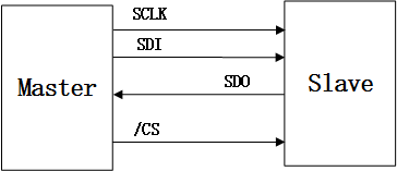
1. Master slave communication
The communication principle of SPI is very simple. It works in the master-slave mode. This mode usually has a master device and one or more slave devices, which need at least 4 lines. In fact, 3 lines can also be used (in one-way transmission). They are common to all SPI based devices. They are SDI (data input), SDO (data output), SCLK (clock) and CS (chip selection).
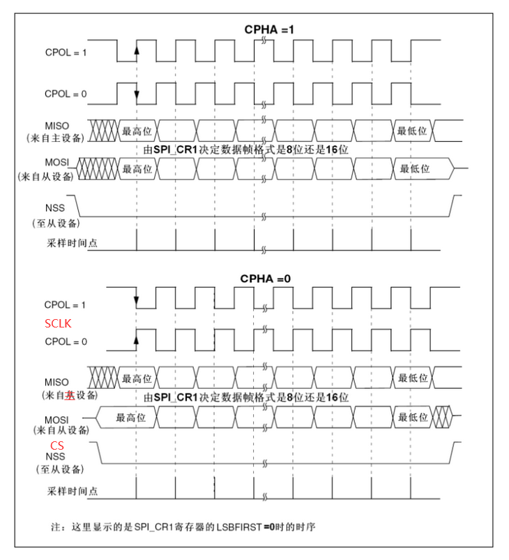
2. Mode selection
SPI communication has four different modes. Different slave devices may be configured to a certain mode at the factory, which cannot be changed; The first mock exam is the same as the two sides of the communication system. But our communication partners must work in the same mode, so we can configure the SPI mode of our main device, and control the communication mode of our main device through CPOL (clock polarity), namely, the level of CPHA idle time and the CPHA (clock phase), the sampling time of data.
The details are as follows:
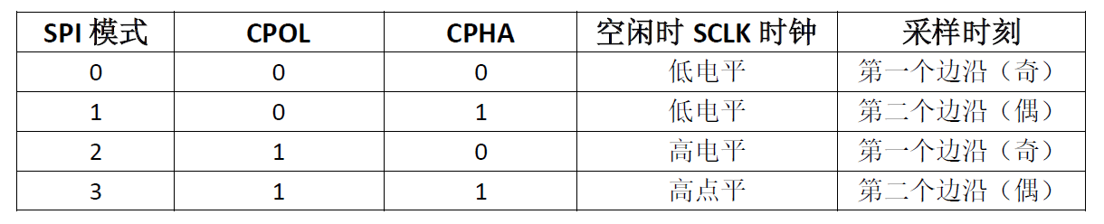
If CPOL is cleared to 0, SCLK remains low in the idle state; otherwise, if it is set to 1, it remains high; If the CPHA bit is cleared to 0, the data bit is sampled at the first edge (odd edge) of each clock cycle of SCLK. Conversely, if it is set to 1, the data bit is sampled at the second edge (even edge) of each clock cycle of SCLK
3, Instance
This example is an example of Tencent classroom SPI interface learned from V3 College - teacher you. The host is FPGA and the slave is DAC3283. Write through FPGA and send data to the slave through SPI protocol to complete one-way communication between the host and the slave (in essence, FPGA configures 32 registers in DAC through this protocol).
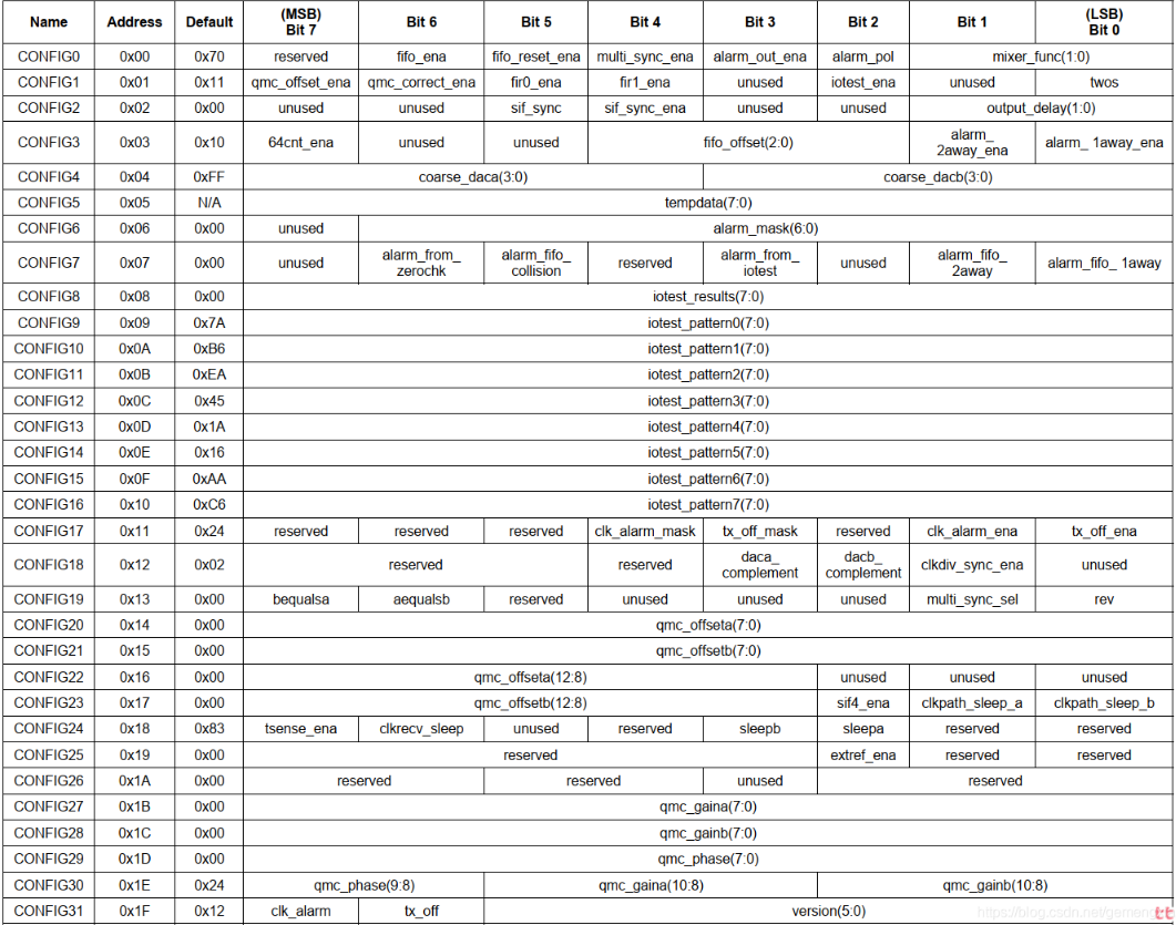
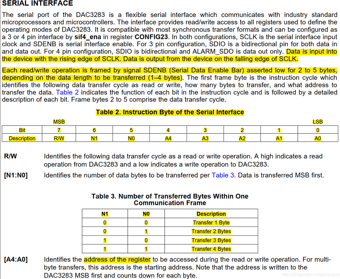
There are 32 registers in DAC3283. The following figure shows the usage rules of each register.
The maximum data that can be written to each register is 5Byte, and the 1Byte is used for command transmission, including read-write control, number of transmitted bytes and register address; The remaining bytes are used for data transmission and register configuration. The command configuration of the first Byte is shown in the following figure:
The following figure shows the sequence diagram of sending the first Byte and the second Byte:
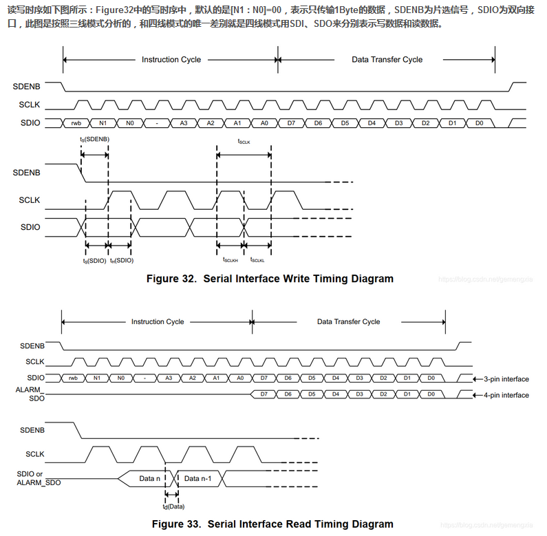
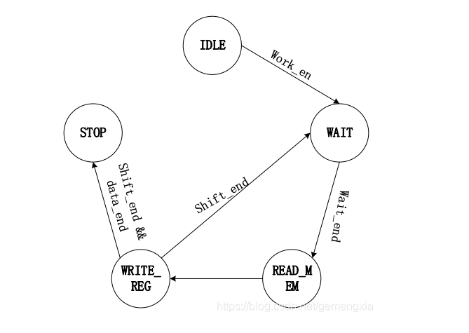
Design process: first, store the command information and data information to be sent in RAM. The depth of ram is 32 (for 32 registers) and the bit width is 16 (8bite command and 8bite data). 16bit information is sent once, 32 times in total. There needs to be a certain time interval between each message sending, so this design adopts the form of state machine. The state machine includes the following five states. It is in IDLE state after power on reset and work_ Pull en high, enter the WAIT state, WAIT for 8 SCLK clock cycles, and then enter READ_MEM state, in which the address of the read ram is accumulated, and the data in the ram is read and stored in the databuff. After waiting for a system cycle, enter WRITE_REG state, in which serial parallel conversion is performed, the data in the databuff is output to spi, and SCLK clock signal and sdenb enable signal are output at the same time. 16 SCLK clock cycles enter the WAIT state for the next data transmission. If it is in write_ If it is detected that all 32 groups of data have been sent in the reg state, it will enter the STOP state. In the design process, it shall be noted that the rising edge of SCLK corresponds to the center position of each data to ensure sufficient establishment time and holding time. The following figure shows the corresponding state transition diagram and Verilog code.
State transition diagram:
Sequence diagram:

Verilog code is as follows:
module  spi_ctrl(
          input              sys_clk,
	  input              sys_res,
	  input              work_en,
//	  input              spo,
	  output     reg     sclk,
	  output     reg     spi,
	  output     reg     sdenb
);
parameter       IDLE = 5'b00001;
parameter       WAIT = 5'b00010;
parameter       READ_MEM = 5'b00100;
parameter       WRITE_REG = 5'b01000;
parameter       STOP = 5'b10000;
reg     [4:0]state;
reg     [4:0]fre_count;
wire          sclk_n;
reg          sclk_p;
reg          sclk_flag;
reg     [3:0]wait_cnt;
reg     [3:0]shift_cnt;//Data shift counter, the first eight bits are command bits and the last eight bits are data bits
reg     [4:0]r_addr;//Read address counter in RAM
reg     [15:0]shift_buff;//Store data read from RAM
reg           data_end;


wire         wren_sig;
wire   [15:0]r_data;


always@(posedge sys_clk or negedge sys_res)begin
     if(!sys_res)
	     fre_count <= 5'd0;
	 else if(fre_count == 5'd24)
	     fre_count <= 5'd0;
	 else
	     fre_count <= fre_count + 1'd1;
end

always@(posedge sys_clk or negedge sys_res)begin
     if(!sys_res)
         sclk_p <= 1'b0;
	 else if(fre_count == 5'd24)
	     sclk_p <= ~sclk_p;
	 else
	     sclk_p <= sclk_p;
end

assign sclk_n = ~sclk_p;

//sclk_flag is the clock SCLK after frequency division_ N flag of one cycle
always@(posedge sys_clk or negedge sys_res)begin
     if(!sys_res)
	    sclk_flag <= 1'b0;
	 else if(fre_count == 5'd24 && sclk_n == 1'b0)
	    sclk_flag <= 1'b1;
	 else
	    sclk_flag <= 1'b0;
end

always@(posedge sys_clk or negedge sys_res)begin
     if(!sys_res)
	wait_cnt <= 4'd0;
     else if(state == WAIT && sclk_flag)
        wait_cnt <= wait_cnt + 1'b1;
     else if(state != WAIT)
        wait_cnt <= 4'd0;
     else
        wait_cnt <= wait_cnt;
end
always@(posedge sys_clk or negedge sys_res)begin
     if(!sys_res)
	shift_cnt <= 4'd0;
     else if(state == WRITE_REG && sclk_flag)
        shift_cnt <= shift_cnt + 1'b1;
     else if(state != WRITE_REG)
        shift_cnt <= 4'd0;
     else
        shift_cnt <= shift_cnt;
end
always@(posedge sys_clk or negedge sys_res)begin
     if(!sys_res)
	    state <= IDLE;
     else begin
        case(state)
		   IDLE:if(work_en)
		           state <= WAIT;
				else
				   state <= state;
		   WAIT:if(wait_cnt[3])
		           state <= READ_MEM;
				else
				   state <= state;
		   READ_MEM:state <= WRITE_REG;
		   WRITE_REG:if(shift_cnt == 4'd15 && sclk_flag && data_end)
						     state <= STOP;
					 else if(shift_cnt == 4'd15 && sclk_flag)
						     state <= WAIT;
					 else
					     state <= state;
		   STOP:state <= state;
           default:state <= IDLE;
        endcase
	 end
end

always@(posedge sys_clk or negedge sys_res)begin
     if(!sys_res)
	    r_addr <= 5'd0;
	 else if(state == READ_MEM)
	    r_addr <= r_addr + 1'b1;
	 else
	    r_addr <= r_addr;
end
always@(posedge sys_clk or negedge sys_res)
      if(!sys_res)
	     data_end <= 1'b0;
	  else if(state == READ_MEM && (&r_addr) == 1'b1)//Equivalent to r_addr == 5‘d31
	     data_end <= 1'b1;
	  else
	     data_end <= data_end;


always@(posedge sys_clk or negedge sys_res)begin
   if(!sys_res)
	    shift_buff <= 16'd0;
	 else if(state == READ_MEM)
	    shift_buff <= r_data;
	 else if(state == WRITE_REG && sclk_flag)
	    shift_buff <= {shift_buff[14:0],1'b1};
	 else
	    shift_buff <= shift_buff;
end

always@(posedge sys_clk or negedge sys_res)
     if(!sys_res)
	    spi <= 1'b0;
	 else if(state == WRITE_REG)
	    spi <= shift_buff[15];
	 else
	    spi <= 1'b0;

always@(posedge sys_clk or negedge sys_res)
      if(!sys_res)
	   sdenb <= 1'b1;
        else if(state == WRITE_REG)
           sdenb <= 1'b0;
        else
           sdenb <= 1'b1;

always@(posedge sys_clk or negedge sys_res)
      if(!sys_res)
	     sclk <= 1'b0;
	  else if(state == WRITE_REG)
	     sclk <= sclk_p;
	  else
	     sclk <= 1'b0;

assign wren_sig = 1'b0;
ram_16_32_r ram_16_32_r_inst (
    .address ( r_addr ),
    .clock ( sys_clk ),
    .data ( 16'd0 ),
    .wren ( wren_sig ),//Write enable high effective, read enable low effective
    .q ( r_data )
    );

endmodule
Simulation verification
tb test code:
`timescale  1ns/1ns
module tb_spi_ctrl;
reg     clk;
reg     res;
reg     work_en;
//wire    spo;
wire    sclk;
wire    spi;
wire    sdenb;
reg     [15:0]read_mem[31:0];
reg     [15:0]shift_buffer = 16'd0;
initial  begin
      clk <= 1'b0;
	  res <= 1'b0;
	  #200 res <= 1'b1;
end

initial  begin
     work_en <= 1'b0;
	 #250 work_en <= 1'b1;
end

initial begin
     $readmemb("ram_data.txt",read_mem);
end
initial begin
    rec_spi();
end


always #10 clk <= ~clk;

task  rec_spi();
   integer  i,j;
   begin

        for(i=0;i<32;i=i+1)begin
		    for(j=0;j<16;j=j+1)begin

			     @(posedge sclk)
				 shift_buffer = {shift_buffer[14:0],spi};
				 if(j == 15 && shift_buffer == read_mem[i])
				      $display("ok,data index is %d,rec_data is %d,send_data is %d",i,shift_buffer,read_mem[i]);
				 else if(j == 15)
				      $display("error");

			end
		end

   end

endtask


  spi_ctrl u_spi_ctrl(
         .sys_clk(clk),
	 .sys_res(res),
	 .work_en(work_en),
	// .spo(spo),
	 .sclk(sclk),
	 .spi(spi),
	 .sdenb(sdenb)
);


endmodule
Read data:
0000000000011111
0000001010011001
0000000000011000
0000001011110110
0001010101000111
0000001001001010
0000001100010001
0010000101111111
0001010101011100
0000011100011100
0000000000000000
0000001100010001
0001011011110011
0000000001010110
0000000000000000
0000001100010001
0010001010101011
0000000000000100
0000001100010001
0001011011100001
1101100111101001
0000000000111000
0000000001010111
0000001101101011
0001111010101110
0000001000111111
0000000111001010
0000000000000000
0000000001010111
0000000001010110
1101010100111011
0000000111001000
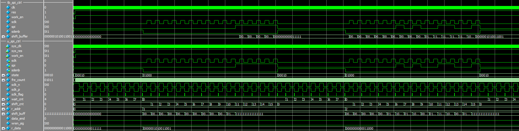
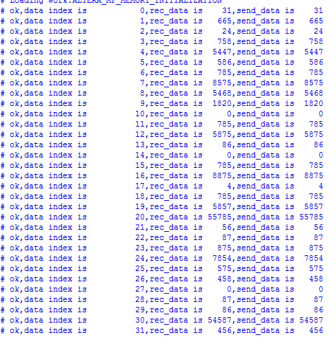
Simulation results (note that since the ramip core is called, the. v file generated by the ramip core and the library file altera_mf.v file need to be added during the simulation):
summary
SPI communication protocol has a wide range of applications. Next, we will continue to learn some examples of this communication protocol, such as full erasure or sector erasure of external Flash within FPGA and the experiment of FPGA reading and writing external Flash.
It is inevitable that there are errors in the article for the first time. I hope readers can correct and give private letters in time. I hope you can make common progress!