testing software: ISE14.7
author: Rose Island
Introduction to APB bus
APB bus
APB(Advanced Peripheral Bus) follows AMBA (Advanced Microcontroller Bus Architecture Protocol). Signal conversion is related to the rising edge of the clock. Each read-write transmission shall be at least two cycles. Read data and write data cannot occur at the same time. APB bridge is the only master device in APB bus, and UART/SPI/I2C are slave devices.
APB interface signal
| APB | Width | Source | Direction | Function |
|---|---|---|---|---|
| pclk | 1 bit | System clock source | input | Clock source of APB bus slave device |
| preset_n | 1 bit | System reset signal | input | System reset |
| rst | 1 bit | Reset signal | input | Slave reset |
| psel | 1 bit | APB Bridge | input | High level indicates that the APB bridge transmits data with the slave device |
| paddr | 10 bits | APB Bridge | input | The corresponding address for reading and writing from the slave device register |
| penable | 1 bit | APB Bridge | input | The read / write enable signal indicates the second clock cycle of an APB transmission and the storage phase |
| pwrite | 1 bit | APB Bridge | input | Indication signal, high write, low read |
| pwdata | 32 bits | APB Bridge | input | Write data |
| prdata | 32 bits | Slave device | output | Read data |
| pready | 1 bit | Slave device | output | When the slave device is ready, it is 1. The slave device can complete transmission at the next rising edge, introduce waiting, and the transmission cycle can be greater than 2 |
Transfer States
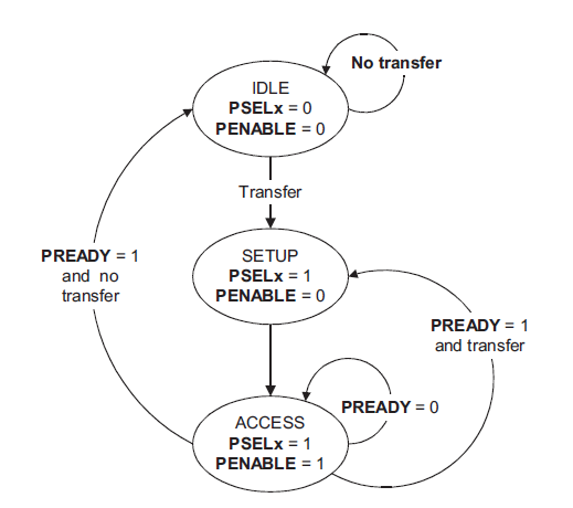
- Setup phase: when data transmission is required, psel is set to 1. There will only be one clock cycle in this phase, and the next rising edge will enter Access phase
- Access phase: the second clock cycle of transmission is set to 1, pwrite/paddr/pwdata/prdata/psel is maintained. Wait for pready. The number of clock cycles in this stage is determined by pready. There is a clock cycle after pready is 1, and then the transmission is completed.
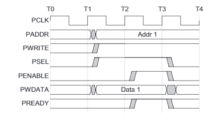
Write data With no wait states
-
APB: T1 (Setup phase): at the rising edge, pwrite outputs 1 (write), paddr outputs write address, pwdata outputs write data, psel outputs 1, penable outputs 0;
T2 (Access phase): penable output 1, pwrite/paddr/pwdata/psel hold;
T3 (Idle phase): penable can output 0 only after the transmission is completed. psel outputs 0 if the next transmission does not arrive immediately.
-
UART: T2: sample write data and update data.
-
Recommendation: pwrite/paddr/pwdata is maintained until the next transmission starts, which can reduce power consumption.
Write data With wait states
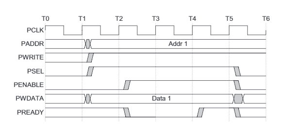
- Pready: output from the slave device. In the Access phase, when penable is high, pready ensures a transmission of at least two clock cycles or longer. Only when pready is high, a transmission is completed.
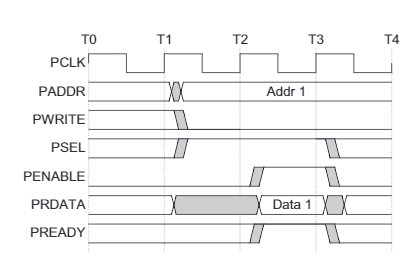
Read data With no wait states
-
APB: T1 (Setup phase): at the rising edge, pwrite outputs 0 (read), paddr outputs write address, psel outputs 1, penable outputs 0;
T2 (Access phase): penable output 1, prdata output write data (provided from the device), pwrite/paddr/psel hold;
T3 (Idle phase): penable can output 0 only after the transmission is completed. psel outputs 0 if the next transmission does not arrive immediately.
-
UART: T2: sample instruction and send read data.
Read data With wait states
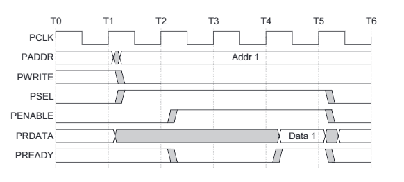
- Ready: output from the slave device. In the Access phase, the transmission cycle can be extended.
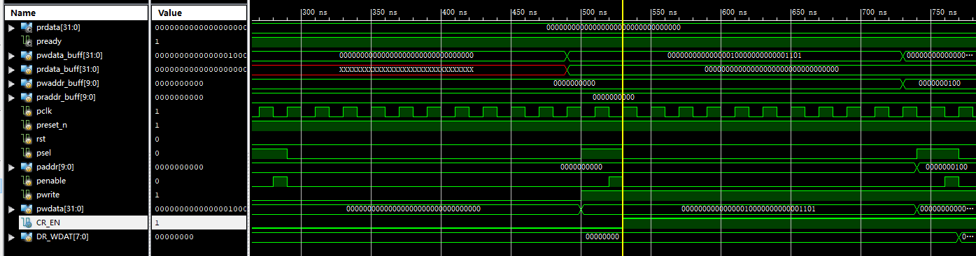
Simulation of APB reading and writing registers
Input excitation
apb signal: pclk, prest_n,rst,psel,paddr,penable,pwrite,pwdata
CSDN's markdown doesn't support verilog code, bad comment! Just make do with the code block of C language
reg [31:0]		pwdata_buff;
reg [31:0]		prdata_buff;

reg [9:0]		pwaddr_buff;
reg [9:0]		praddr_buff;

// input
reg				pclk;
reg				preset_n;
reg				rst;
reg				psel;
reg [9:0]		paddr;
reg				penable;
reg				pwrite;
reg [31:0]		pwdata;

// output
wire [31:0]		prdata;
wire			pready;

task apb_write(input [9:0] addr, input [31:0] data);
begin
	@(negedge pclk);
		psel	= 1'b1;
		penable	= 1'b0;
		pwrite	= 1'b1;
		paddr	= addr;
		pwdata	= data;
	@(posedge pclk);

	@(negedge pclk);
		penable	= 1'b1;
	@(posedge pclk);

	while(pready != 1'b1) @(posedge pclk);
		psel	= 1'b0;
		penable	= 1'b0;
		// pwrite	= 1'b0;
		// paddr	= 32'b0;
		// pwdata	= 32'b0;
	repeat (10) @(posedge pclk);
end
endtask //apb_write

task apb_read(input [9:0] addr, output [31:0] data);
begin
	@(negedge pclk);
		psel	= 1'b1;
		penable	= 1'b0;
		pwrite	= 1'b0;
		paddr	= addr;
	@(posedge pclk);

	@(negedge pclk);
		penable = 1'b1;
	@(posedge pclk);

	while(pready != 1'b1) @(posedge pclk);
		data	= prdata;
		psel	= 1'b0;
		penable	= 1'b0;
		// pwrite	= 1'b0;
		// paddr	= 32'b0;
	repeat(10) @(posedge pclk);
end
endtask //apb_read

initial begin
	pwaddr_buff = 10'h000;
	pwdata_buff = 32'b1101;
	apb_write(pwaddr_buff,pwdata_buff);

	praddr_buff = 10'h000;
	apb_read(praddr_buff,prdata_buff);
	if(prdata_buff == 32'b1101) begin
		$display("\n ------ write and read successfully -------");
	end
	else begin
		$display("\n ------ write or read failed -------");
	end
end
Observation signal
- Write data: e.g. write CR register and observe CR_ Is the en bit set to 1
- Read data: e.g. read the value in CR register
wave form
-
Write data: e.g. CR_EN
-
Read data: e.g. read CR register
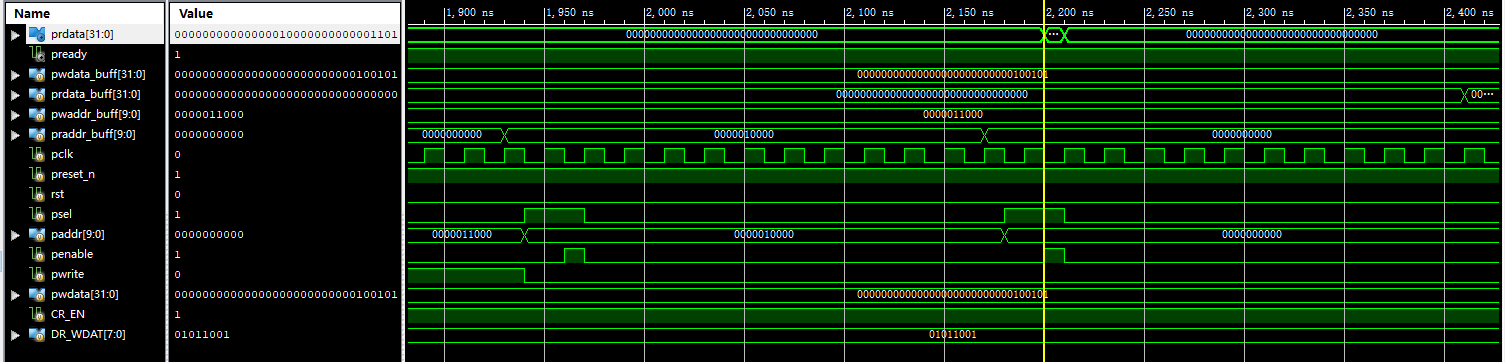
Actual results
- Write successfully, pass √
- Read successfully, pass √