HDLBits-Karnaugh Map to Circuit
Problem 72 3-variable
Requirement:
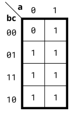
The circuit is realized according to the Karnaugh diagram, and the circuit design is completed in the form of the sum of the product of the maximum term and the minimum term. Before writing verilog, you can simplify the Karnaugh map.
Solution:
module top_module(
    input a,
    input b,
    input c,
    output out  );

    assign out = a | b | c;

endmodule
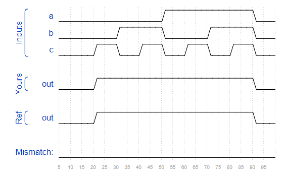
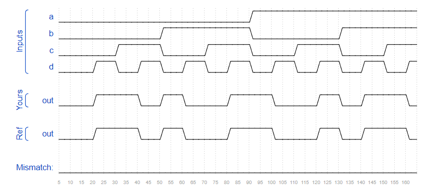
Timing Diagram:
Problem 73 4-variable
Requirement:
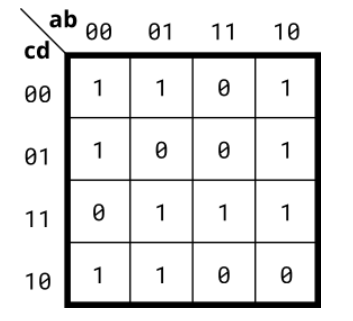
According to the Karnaugh diagram to design the circuit, this topic is 4 variables.
Solution:
module top_module(
    input a,
    input b,
    input c,
    input d,
    output out  );

    assign out = (!a & !d) | (d & a & !b) | (b & c & d) | (a & !b & !c & !d) | (!a & !b & !c & d);

endmodule
PS: the simplification here is not accurate enough. There can be repeated parts when drawing circles.
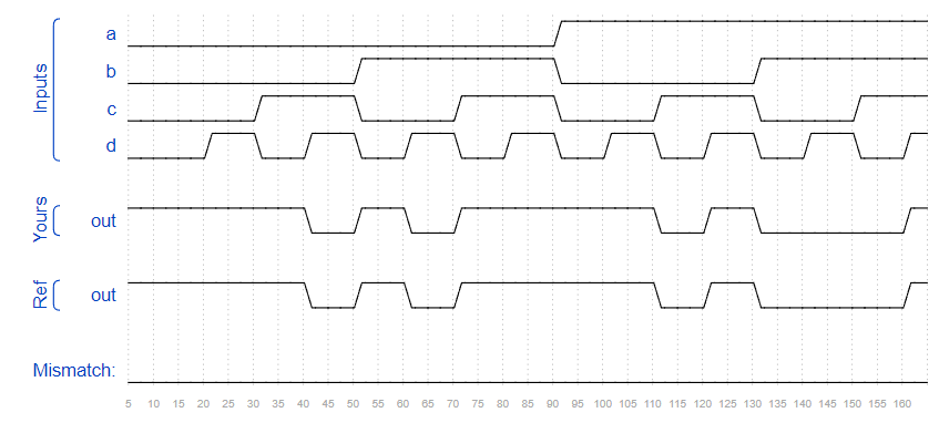
Timing Diagram:
Problem 74 4-variable
Requirement:
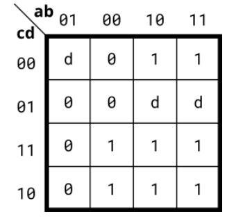
According to the Karnaugh diagram, the following circuits are realized:
Solution:
module top_module(
    input a,
    input b,
    input c,
    input d,
    output out  );

    assign out = a | (!b & c);

endmodule
PS:
Where D is the don't care value, which is equivalent to X. any value that is convenient for simplification can be selected (circle or not).
If the product of the largest term is used, it is: assign out = (a|c) & (a| ~ b);
Missed: ab is not the order of 00 → 01 → 11 → 10!!! The Karnaugh map idea ensures that the variables adjacent to the space are logically adjacent. Only one bit of 01 → 00 → 10 → 11 changes each time, so it is logically adjacent.
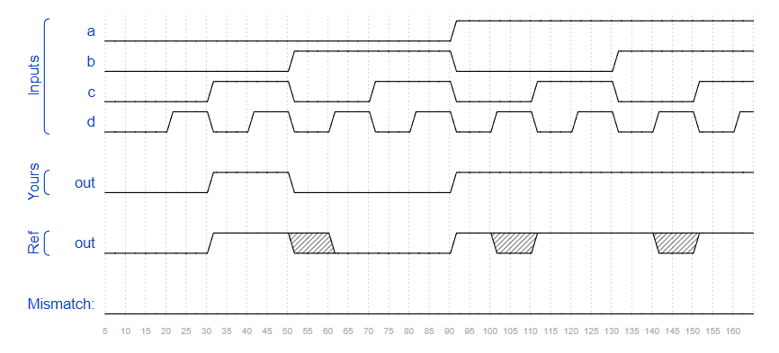
Timing Diagram:
Problem 75 4-variable
Requirement:
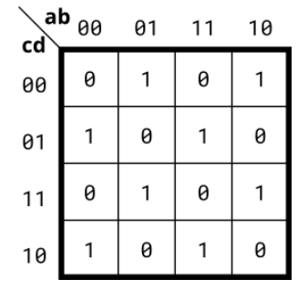
Realize the circuit according to the Karnaugh diagram:
Solution:
module top_module(
    input a,
    input b,
    input c,
    input d,
    output out  );

    assign out = a^b^c^d;

endmodule
PS: it's a representative Karnaugh map.
Timing Diagram:
Problem 76 Minimum SOP and POS
Requirement:
A logic circuit with four inputs a, b, c, d and one output. When the input is 2, 7 or 15, the output is 1, when the input is 0, 1, 4, 5, 6, 9, 10, 13 or 14, the output is 0, and when the input is 3, 8, 11 or 12, the output is any value. For example, 7 corresponds to the input abcd of 0, 1, 1, 1.
Note: SOP and POS of the circuit must be the minimum value after simplification
Solution:
module top_module (
    input a,
    input b,
    input c,
    input d,
    output out_sop,
    output out_pos
);

    assign out_sop = (c&d) | (!a&!b&c);
    assign out_pos = c & (!a|d) & (!b|d);

endmodule
PS: SOP and POS
The sum of the products of sop, sum of product is the form of the smallest term.
The product of pos, product of sum, that is, the form of the largest term.
Miss: parentheses can't be used casually. A | (B & C) is different from a | (B & C).
Problem 77 Karnaugh map
Requirement:
Realize the circuit according to the Karnaugh diagram:
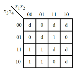
Solution:
module top_module (
    input [4:1] x,
    output f );

    assign f = (!x[1]&x[3]) | (x[2]&!x[3]&x[4]);

endmodule
Problem 78 Karnaugh map
Requirement:
Or draw the circuit according to Kano's picture:
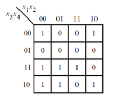
Solution:
module top_module (
    input [4:1] x,
    output f);

    assign f = (!x[1]&x[3])|(x[1]&!x[2]&!x[4])|(!x[2]&!x[3]&!x[4])|(x[1]&x[2]&x[3]&x[4]);

endmodule
Problem 79 K-map implemented with a multiplexer
Requirement:
According to the Karnaugh diagram given in the title, a 4-1 multiplexer and as many 2-1 multiplexers as possible are used to realize the circuit. Other logic gates are not allowed, and ab must be used as the input of the selector. Just implement the tag top_module, the whole circuit (including 4-to-1 multiplexer) to realize Karnaugh map.
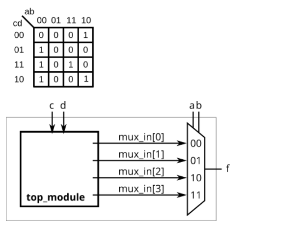
Solution:
module top_module (
    input c,
    input d,
    output [3:0] mux_in
);

    assign mux_in[0] = c|d;
    assign mux_in[1] = 1'b0;
    assign mux_in[3] = c&d;
    assign mux_in[2] = (!c&!d)|(c&!d);

endmodule
Missed: 11 corresponds to the third column, not the fourth column.
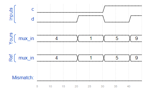
Timing Diagram:
Don't want to learn ORZ (it's no good. Hello (# ` O ')
