Implementation principle reference: Asynchronous fifo -- Verilog implementation_ Alan aixiao's blog - CSDN blog_ Asynchronous fifo
Code reference: IC Foundation (I): asynchronous fifo_ Maochuang an's blog - CSDN blog_ Asynchronous fifo
1. Key points of asynchronous FIFO design:
(1) Conversion from binary code to gray code:
The highest bit of the binary code remains unchanged, and the other bits are XOR with the left bit to get the gray code. That is, move the binary code one bit to the right and XOR with yourself to get the corresponding gray code.
Namely: assign gray = ( bin >> 1 ) ^ bin ;
(2) Synchronization of clock domain:
The gray code corresponding to the binary address is delayed by the synchronization module from the FIFO empty module to the FIFO full module to complete the clock synchronization. The same goes for the full module to the empty module.
(3) Logic of FIFO full and empty judgment through gray code:
Full judgment: the highest and second highest positions are different, and others are the same. Namely:
assign wfull_val = ( wgraynext == { ~wq2_rptr [ ADDR_SIZE: ADDR_SIZE - 1 ], wq2_rptr [ ADDR_SIZE-2: 0 ] } )Full judgment: Gray code is exactly the same. Namely:
assign rempty_val = ( rgraynext == rq2_wptr );
2. Function of each module and detailed explanation of Verilog code:
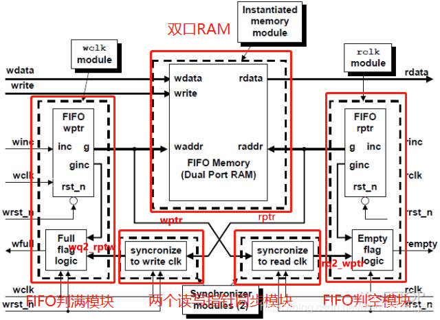
(the picture is taken from the blog at the beginning, with changes)
(1) Dual port RAM module
Function: as an enclosure, the input read and write addresses are binary. The highest bit is used to store empty / full signals.
Port Description:
wclken: Write enable
wclk: Write clock
raddr: Read address
waddr: Write address
wdata: Data written to RAM
rdata: Data read from RAM
module DualRAM #(
    parameter           DATA_SIZE = 8,       // Data bit width
    parameter           ADDR_SIZE = 4        // FIFO address depth
    )(
    input                       wclken,      // Write enable
    input                       wclk,        // Write clock
    input  [ADDR_SIZE - 1: 0]   raddr,       // Read address
    input  [ADDR_SIZE - 1: 0]   waddr,       // Write address
    input  [DATA_SIZE - 1: 0]   wdata,       // Data written to RAM
    output [DATA_SIZE - 1: 0]   rdata        // Data read from RAM
    );

    localparam RAM_DEPTH = 1 << ADDR_SIZE;   // RAM depth, the highest bit stores the empty and full signal pointer

    reg [DATA_SIZE-1: 0] mem [0:RAM_DEPTH-1];// Open up memory

    // Write timing
    always @ ( posedge wclk ) begin
        if ( wclken == 1'b1 ) begin
            mem[ waddr ] <= wdata;           // Write enable signal is high, write data
        end

        else begin
            mem[ waddr ] <= mem[ waddr ];    // Write enable didn't come, keep it
        end
    end

    assign      rdata   =  mem [ raddr ];    // Read the address and give the data directly

endmodule
(2) FIFO empty module
Function: input the read enable signal, generate the corresponding binary address and output it to the RAM module, convert the binary address into the corresponding gray code and output it to the synchronization module, which synchronizes the read address to the write clock domain.
Note that the signal transmitted from the module to the synchronization module in the figure is the gray code corresponding to the binary address.
Port Description:
rclk : Read clock signal
rinc : Read enable signal. For each read enable signal, add one to the read address
rrst_n: Reset signal
rq2_wptr: write pointer code passed in by synchronization module
rempty : Output FIFO null signal
raddr : Binary read address output to RAM
rptr : Gray code output to write clock field
module rptr_empty # (
    parameter   ADDR_SIZE = 4
)
(
    input                           rclk,
    input                           rinc,       // Read enable signal: add one to the read address for each read enable signal
    input                           rrst_n,
    input       [ ADDR_SIZE    :0 ] rq2_wptr,   // Write pointer code passed in by synchronization module
    output reg                      rempty,
    output      [ ADDR_SIZE - 1:0 ] raddr,      // Read address output to RAM
    output reg  [ ADDR_SIZE    :0 ] rptr        // Gray code output to the write clock field: one more bit than the address, and the highest bit is used to judge the empty and full state
    );

    reg     [ ADDR_SIZE: 0 ]    rbin;           // Binary address
    wire    [ ADDR_SIZE: 0 ]    rgraynext, rbinnext;    // Binary and gray code addresses
    wire                        rempty_val;

    //----------Address logic-------------//

    always @ ( posedge rclk or negedge rrst_n ) begin
        if ( !rrst_n ) begin
            rbin <= 0;
            rptr <= 0;
        end
        else begin
            rbin <= rbinnext;       // Clock to update the binary address
            rptr <= rgraynext;      // Update the gray code of the corresponding address
        end
    end

    // Address generation logic
    assign rbinnext = !rempty ? ( rbin + rinc ): rbin;      // Binary address update logic: if FIFO is not empty, the address is current address + read enable (i.e. address plus one); If FIFO is empty, the address will not be updated
    assign rgraynext = ( rbinnext >> 1 ) ^ ( rbinnext );    // Gray code address generation: XOR after binary is shifted one bit to the right
    assign raddr = rbin[ ADDR_SIZE - 1: 0 ];                // Read address into RAM

    // FIFO empty judgment
    assign rempty_val = ( rgraynext == rq2_wptr );          // Null determination logic: if the gray code of the write pointer is exactly the same as the gray code of the read pointer, it is null


    // Judgment sequence of empty signal rempty
    always @ ( posedge rclk or negedge rrst_n ) begin
        if ( !rrst_n )
            rempty <= 1'b1;                 // When reset, FIFO is empty
        else
            rempty <= rempty_val;           // Need another signal rempty_val write timing logic
    end

endmodule
(3) Read clock domain to write clock domain synchronization module
Function: delay the gray code address generated by FIFO blank judgment module by one beat, and then output the address to the write clock field.
Port Description:
rptr : Gray code address pointer passed in by null determination module
wclk : External incoming write clock signal
wrst_n: External incoming write reset signal
wq2_rptr: Gray code address pointer output to the full judgment module
module sync_r2w # (
    parameter       ADDR_SIZE = 4
)
(
    input       [ ADDR_SIZE: 0 ]    rptr,       // Gray code address pointer passed in by null determination module
    input                           wclk,       // External incoming write clock signal
    input                           wrst_n,     // External incoming write reset signal
    output  reg [ ADDR_SIZE: 0 ]    wq2_rptr    // Gray code address pointer output to full judgment module
    );

    reg [ ADDR_SIZE: 0 ]    wq1_rptr;           // This register is used to generate a delay of one beat

    // D trigger, two-stage synchronization
    always @ ( posedge wclk or negedge wrst_n ) begin
        if ( !wrst_n )
            { wq2_rptr, wq1_rptr } <= 0;
        else                                                    // It is equivalent to delaying the input address by one clock cycle:
            { wq2_rptr, wq1_rptr } <= { wq1_rptr, rptr };       // In the first cycle, the address pointer of the empty judgment module is given to the beat register, and in the second cycle, it is taken out to the output signal
    end

endmodule
(4) The full rating module is the same as another synchronization module, and the code is pasted directly:
Full rating module:
module wptr_full# (
    parameter   ADDR_SIZE = 4
)
(
    input                           wclk,
    input                           winc,
    input                           wrst_n,
    input       [ ADDR_SIZE    :0 ] wq2_rptr,
    output reg                      wfull,
    output      [ ADDR_SIZE - 1:0 ] waddr,      // Read address output to RAM
    output reg  [ ADDR_SIZE    :0 ] wptr        // Gray code output to write clock field
    );

    reg     [ ADDR_SIZE: 0 ]    wbin;           // Binary address
    wire    [ ADDR_SIZE: 0 ]    wgraynext, wbinnext;    // Binary and gray code addresses
    wire                        wfull_val;

    //----------Address logic-------------//

    always @ ( posedge wclk or negedge wrst_n ) begin
        if ( !wrst_n ) begin
            wbin <= 0;
            wptr <= 0;
        end
        else begin
            wbin <= wbinnext;
            wptr <= wgraynext;
        end
    end

    // Address generation logic
    assign wbinnext = !wfull ? ( wbin + winc ): wbin;
    assign wgraynext = ( wbinnext >> 1 ) ^ ( wbinnext );
    assign waddr = wbin[ ADDR_SIZE - 1: 0 ];

    // FIFO full
    assign wfull_val = ( wgraynext == { ~wq2_rptr [ ADDR_SIZE: ADDR_SIZE - 1 ], wq2_rptr [ ADDR_SIZE-2: 0 ] } );//The highest two digits are reversed and then judged

    always @ ( posedge wclk or negedge wrst_n ) begin
        if ( !wrst_n )
            wfull <= 1'b0;
        else
            wfull <= wfull_val;
    end
endmodule
Synchronization module:
// The write pointer is synchronized to the read clock module
module sync_w2r # (
parameter ADDR_SIZE = 4
)
(
input [ ADDR_SIZE: 0 ] wptr, // Write address gray code generated by full judgment module
input rclk,
input rrst_n,
output reg [ ADDR_SIZE: 0 ] rq2_wptr // Write address code output to read clock field
);
reg [ ADDR_SIZE: 0 ] rq1_wptr; // One shot delay
// D trigger, two-stage synchronization
always @ ( posedge rclk or negedge rrst_n ) begin
if ( !rrst_n )
{ rq2_wptr, rq1_wptr } <= 0;
else
{ rq2_wptr, rq1_wptr } <= { rq1_wptr, wptr }; // It is equivalent to delaying the input address by one clock cycle
end
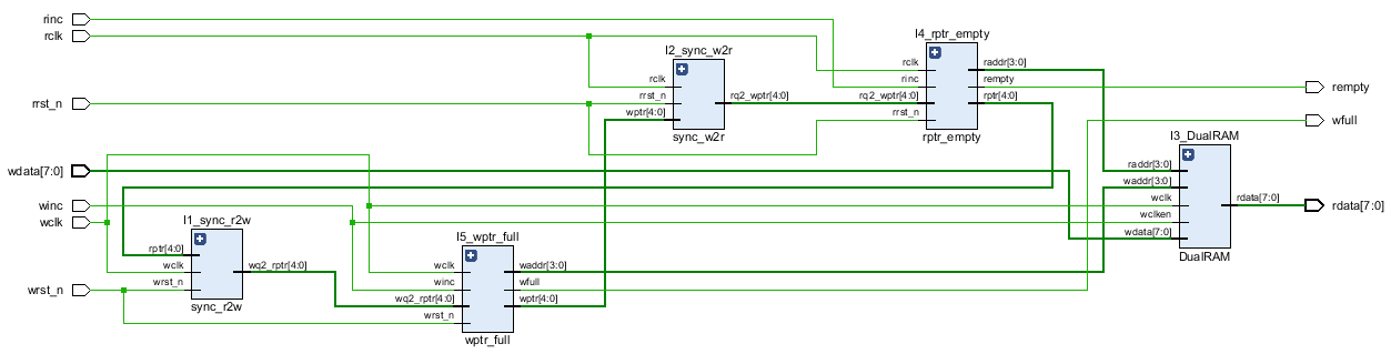
endmodule(5) Connect the top module:
module AsyncFIFO # (
    parameter   ADDR_SIZE = 4,
    parameter   DATA_SIZE = 8
    )
(
    input       [ DATA_SIZE - 1: 0 ]    wdata,
    input                               winc,
    input                               wclk,
    input                               wrst_n,
    input                               rinc,
    input                               rclk,
    input                               rrst_n,
    output      [ DATA_SIZE - 1: 0 ]    rdata,
    output                              wfull,
    output                              rempty
    );

    wire        [ ADDR_SIZE - 1: 0 ]     waddr, raddr;
    wire        [ ADDR_SIZE    : 0 ]     wptr, rptr, wq2_rptr, rq2_wptr;


    sync_r2w # (
    .ADDR_SIZE ( ADDR_SIZE )
)
    I1_sync_r2w (
        .rptr       ( rptr      ),
        .wclk       ( wclk      ),
        .wrst_n     ( wrst_n    ),
        .wq2_rptr   ( wq2_rptr  )
    );


    sync_w2r # (
    .ADDR_SIZE ( ADDR_SIZE )
)
    I2_sync_w2r (
        .wptr       ( wptr      ),
        .rclk       ( rclk      ),
        .rrst_n     ( rrst_n    ),
        .rq2_wptr   ( rq2_wptr  )
    );


    DualRAM # (
    .DATA_SIZE ( DATA_SIZE ),           // Data bit width
    .ADDR_SIZE ( ADDR_SIZE )            // FIFO address depth
    )
        I3_DualRAM (
        .wclken     ( winc      ),      // Write enable
        .wclk       ( wclk      ),      // Write clock
        .raddr      ( raddr     ),      // Read clock
        .waddr      ( waddr     ),      // Write address
        .wdata      ( wdata     ),      // Data written to RAM
        .rdata      ( rdata     )       // Data read from RAM
    );


    rptr_empty # (
    .ADDR_SIZE ( ADDR_SIZE )
    )
        I4_rptr_empty (
        .rclk       ( rclk      ),
        .rinc       ( rinc      ),
        .rrst_n     ( rrst_n    ),
        .rq2_wptr   ( rq2_wptr  ),
        .rempty     ( rempty    ),
        .raddr      ( raddr     ),      // Read address output to RAM
        .rptr       ( rptr      )        // Gray code output to write clock field
    );


    wptr_full# (
   .ADDR_SIZE ( ADDR_SIZE )
    )
       I5_wptr_full  (
        .wclk       ( wclk      ),
        .winc       ( winc      ),
        .wrst_n     ( wrst_n    ),
        .wq2_rptr   ( wq2_rptr  ),
        .wfull      ( wfull     ),
        .waddr      ( waddr     ),      // Read address output to RAM
        .wptr       ( wptr      )        // Gray code output to write clock field
    );

endmodule
(6)testbench
module tb();

parameter		DATA_SIZE = 16;
parameter		ADDR_SIZE = 16;


reg  [ DATA_SIZE - 1: 0]    wdata;
reg                         winc, wclk, wrst_n;
reg                         rinc, rclk, rrst_n;
wire [ DATA_SIZE - 1: 0 ]   rdata;
wire                        wfull;
wire                        rempty;
integer		                i=0;

AsyncFIFO # (
    .ADDR_SIZE ( ADDR_SIZE ),
    .DATA_SIZE ( DATA_SIZE )
)
u_fifo (
               .rdata   ( rdata     ),
               .wfull   ( wfull     ),
               .rempty  ( rempty    ),
               .wdata   ( wdata     ),
               .winc    ( winc      ),
               .wclk    ( wclk      ),
               .wrst_n  ( wrst_n    ),
               .rinc    ( rinc      ),
               .rclk    ( rclk      ),
               .rrst_n  ( rrst_n    )
 );
localparam CYCLE = 20;
localparam CYCLE1 = 40;

            initial begin
                wclk = 0;
                forever
                # ( CYCLE / 2 )
                wclk =~ wclk;
            end

            initial begin
                rclk = 0;
                forever
                # ( CYCLE1 / 2)
                rclk =~ rclk;
            end

            initial begin
                wrst_n = 1;
                #2;
                wrst_n = 0;
                # ( CYCLE * 3 );
                wrst_n = 1;
            end

             initial begin
                rrst_n = 1;
                #2;
                rrst_n = 0;
                # ( CYCLE * 3 );
                rrst_n = 1;
            end

            always  @ ( posedge wclk or negedge wrst_n ) begin
                if ( wrst_n == 1'b0 ) begin
                    i <= 0;
                end
                else if ( !wfull ) begin
                    i = i+1;
                end
                else begin
                	i <= i;
                end
            end

            always  @ ( rempty or rrst_n ) begin
                if ( rrst_n == 1'b0 ) begin
                    rinc = 1'b0;
                end
                else if ( !rempty ) begin
                    rinc = 1'b1;
                end
                else
                	rinc = 1'b0;
            end

            always @ ( wfull or wrst_n ) begin
	           if ( wrst_n )
		          winc = 1'b0;
	           if ( !wfull )
		          winc = 1'b1;
	           else
		          winc = 1'b0;
            end

            always @ ( * ) begin
                if ( !wfull )
                    wdata = i;
                else
                    wdata = 0;
            end

endmodule
RTL diagram:
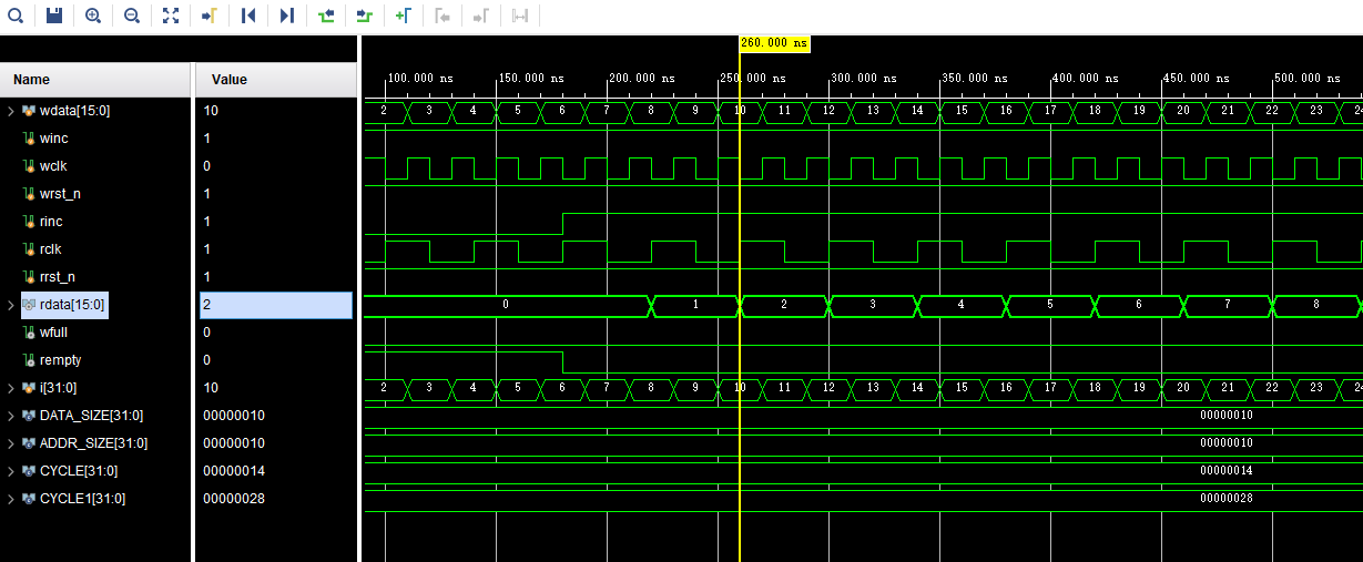
Simulation diagram: