catalogue
5. Preparation of program code
6. Configure corresponding pins
Statement: the FPGA development board I bought is Heijin AX4010 series, and the model is EP4CE10F17C8N. I study with Heijin community step by step. Taking notes is to summarize and summarize and facilitate my later learning partners. The author's style is similar to that of Heijin community (after all, learning with is a shadow). The article [FPGA series from 0] is limited to learning and is not allowed to be used for commercial purposes, Reprint please indicate the author and source! Thanks, the code is not easy!
1. Experimental purpose
This experiment describes how to build the project step by step in quartus13.1, configure the pins, compile and download them to the development board EP4CE10F17C8N. The program turns on four LED s every 1s to form a running light.
2. Preparation stage
2.1 computer installation Quartus13.1 software
2.2 the FPGA development board is black gold AX4010 series, and the model is EP4CE10F17C8
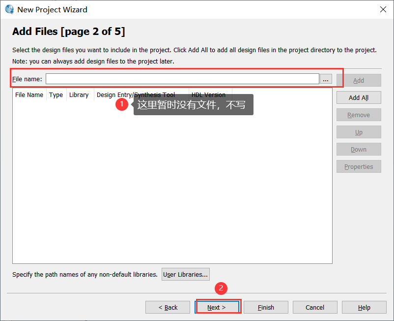
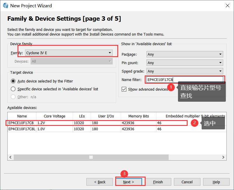
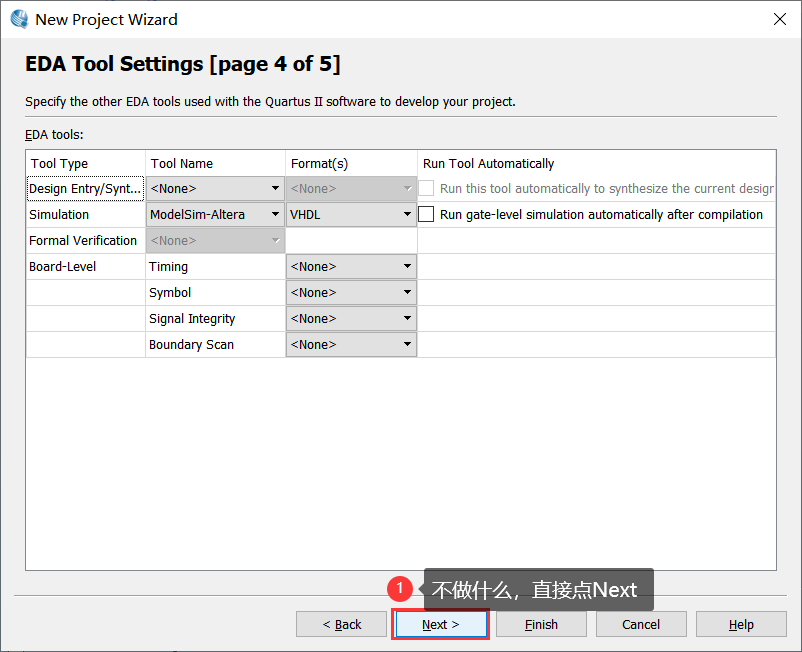
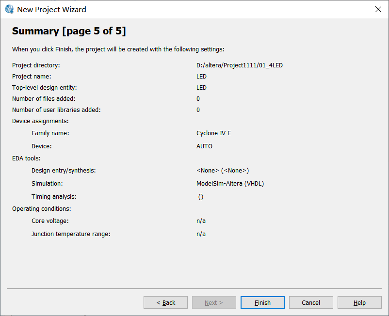
3. Establish project
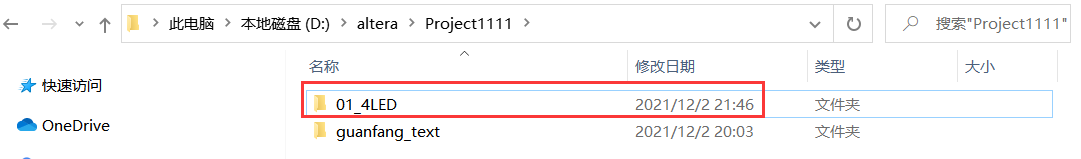
By default, quartus 13.1 is ready to be installed and cracked, and a 01 is created in disk D (optional)_ 4led files store engineering files (Note: files cannot contain Chinese and spaces)
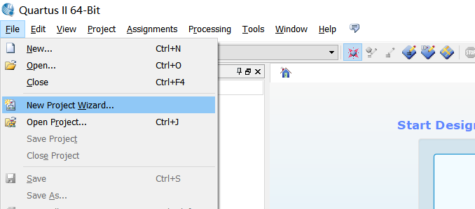
Open quartus 13.1 and click file -- > new project wizard
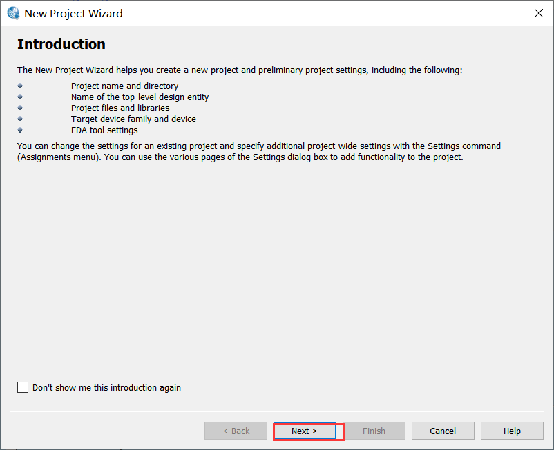
Click Next
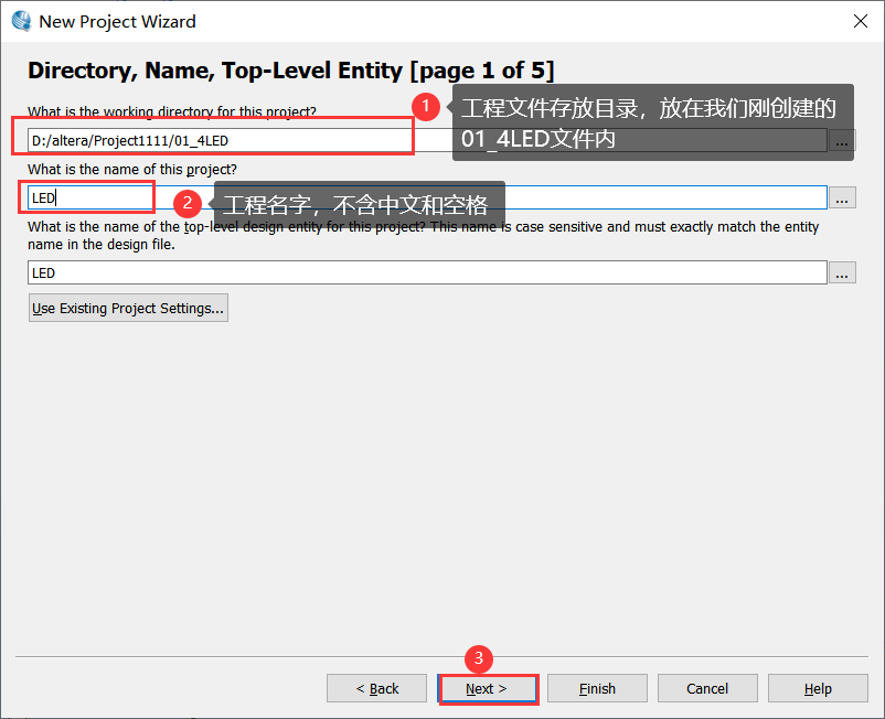
The summary of the project file information written above is used for inspection, and click Finish
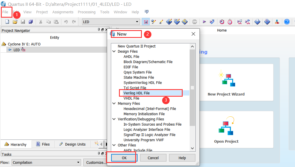
4. Create Verilog HDL File
Click file - > New - > Verilog HDL file - > OK
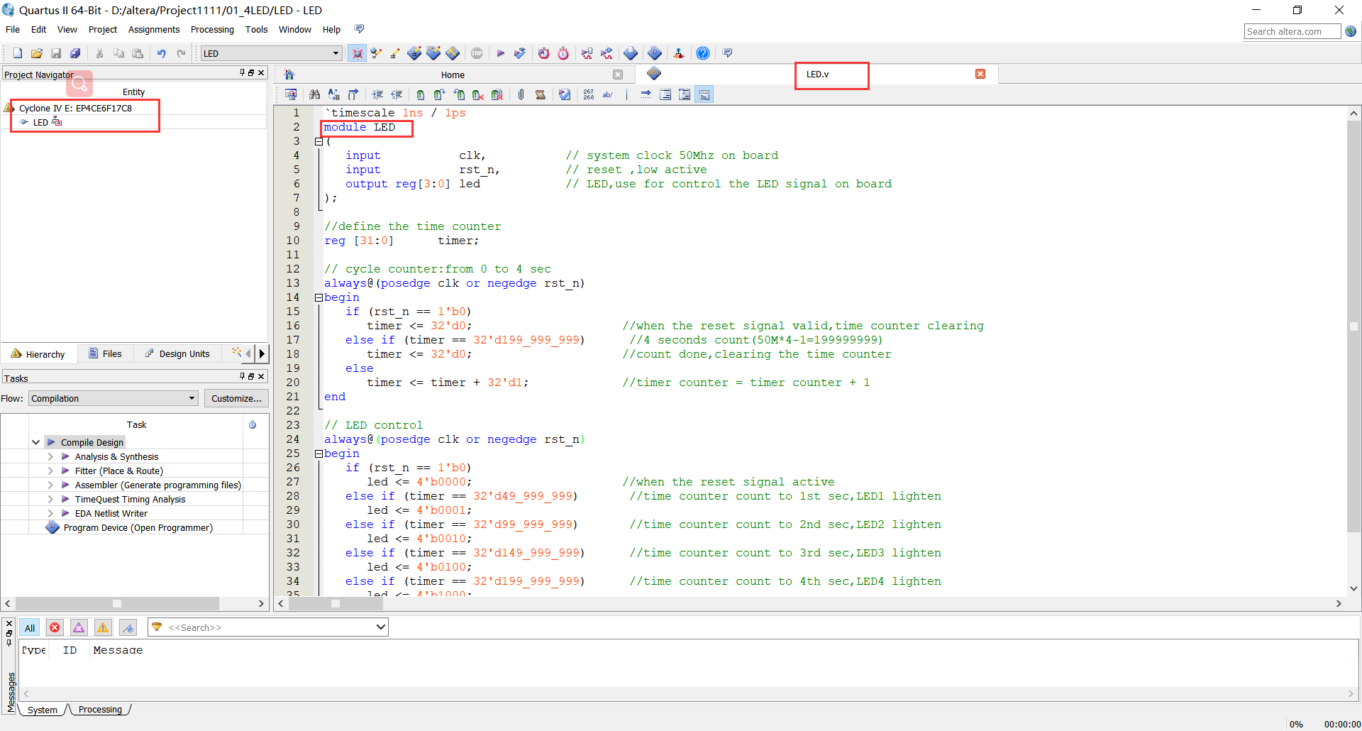
5. Preparation of program code
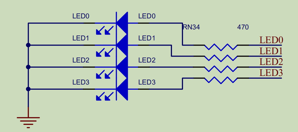
Check the schematic diagram of board EP4CE10F17C8. It is known that LED0, LED1, LED2 and LED3 are common negative, and the high level is effective, that is, the high level is on. (each hardware development board is different, and the program is adjusted according to its own schematic diagram)
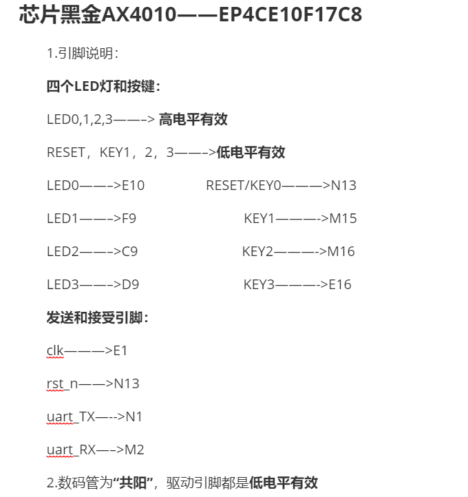
I summarized the pin distribution of FPGA black gold AX4010 series EP4CE10F17C8
Write the program (from the matching routine of the black gold board):
`timescale 1ns / 1ps
module LED
(
	input           clk,           // system clock 50Mhz on board
	input           rst_n,         // reset ,low active
	output reg[3:0] led            // LED,use for control the LED signal on board
);

//define the time counter
reg [31:0]      timer;

// cycle counter:from 0 to 4 sec
always@(posedge clk or negedge rst_n)
begin
	if (rst_n == 1'b0)
		timer <= 32'd0;                     //when the reset signal valid,time counter clearing
	else if (timer == 32'd199_999_999)      //4 seconds count(50M*4-1=199999999)
		timer <= 32'd0;                     //count done,clearing the time counter
	else
		timer <= timer + 32'd1;             //timer counter = timer counter + 1
end

// LED control
always@(posedge clk or negedge rst_n)
begin
	if (rst_n == 1'b0)
		led <= 4'b0000;                     //when the reset signal active
	else if (timer == 32'd49_999_999)       //time counter count to 1st sec,LED1 lighten
		led <= 4'b0001;
	else if (timer == 32'd99_999_999)       //time counter count to 2nd sec,LED2 lighten
		led <= 4'b0010;
	else if (timer == 32'd149_999_999)      //time counter count to 3rd sec,LED3 lighten
		led <= 4'b0100;
	else if (timer == 32'd199_999_999)      //time counter count to 4th sec,LED4 lighten
		led <= 4'b1000;
end
endmodule
Note: the two should be consistent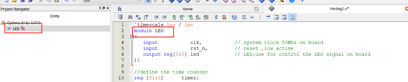
Write the program and save it as LED.v file
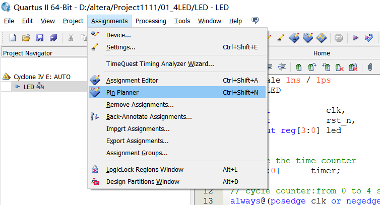
6. Configure corresponding pins
Click assignments - > pin planner to configure pins. The purpose of pin assignment is to associate the design with the actual hardware circuit.
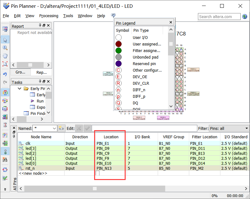
It can be seen from the schematic diagram that for the pin corresponding to each LED lamp, write the pin name at the Location and press enter, as shown in the figure. It should be noted that each IO must be assigned a pin. If there is an unallocated IO, the software may be randomly assigned, resulting in unpredictable consequences. In serious cases, the FPGA chip can be burned out
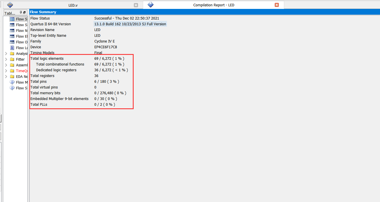
Then compile the project file and click processing - > start compilation
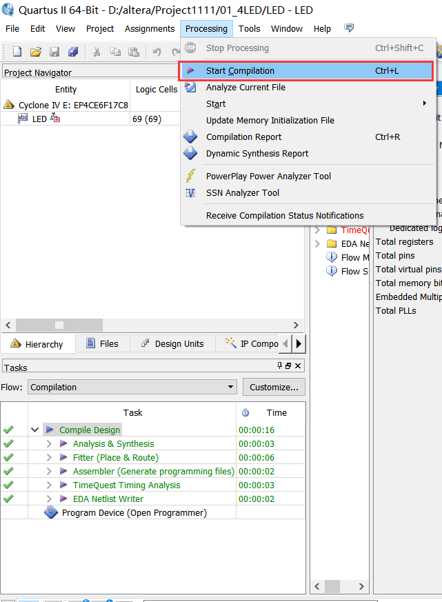
Then, if the compilation is successful, the Report of how many resources of FPGA are occupied by the project file will be printed.
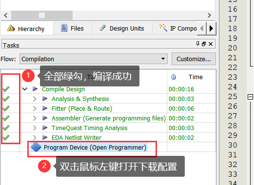
7. Program Download Board
Click Hardware Setup and select USB blaster [usb-0], Select JTAG download, click Add File, and select output in the project file_ Files file, and then click Start to download. The LED.sof file can be downloaded to FPGA through JTAG, but it cannot be directly solidified to Flash.
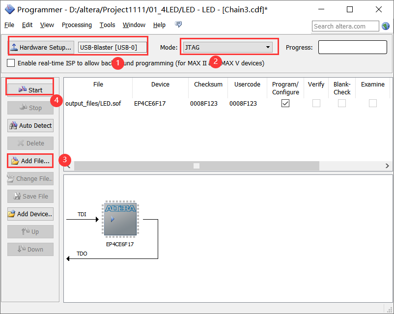
A green Successful download appears.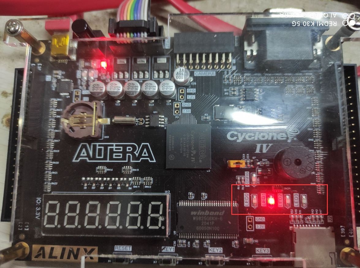
Observe the development board phenomenon:
8. Curing program to Flash