The book continues from the above. The previous article introduced the slightly simple synchronous fifo, and then began the more complex asynchronous fifo.
1. Difference between synchronous fifo and asynchronous fifo
When there is only one clock in the design, whether all registers use the same one, there will be no transmission speed mismatch; However, when there are multiple clock signals in the design and data is transmitted in these clock domains, data loss may occur due to clock signal mismatch. At this time, asynchronous fifo needs to cache data to ensure normal data transmission. Therefore, generally asynchronous fifo will include a dual port ram
2. Asynchronous fifo composition
Figure 1. Asynchronous fifo
Module composition (6): top-level module, dual port RAM, 2 cross clock domain synchronous pointer modules, null judgment logic and full judgment logic.
3. Precautions
1) Avoid using binary counters to implement pointers, because if the current value is carried by one, all bits may change, and the error rate may increase. eg:0111 plus 1 will become 1000, and three of them will change, so the error rate will be increased.
2) To solve the above problems, it is recommended to directly use gray code counting.
3) Define more than one bit of the pointer's bit width. For example, suppose you want to design an asynchronous FIFO with a depth of 8. At this time, only 3 bits (2 ^ 3 = 8) are needed to define the read-write pointer. However, we design the pointer's bit width to 4 bits in the design. The function of the highest bit is to distinguish whether to read null or write full. Specific theory 1 As follows, when the highest bit is the same, the other bits are the same, it is considered to be read empty; When the highest bit is different and the other bits are the same, it is considered to be full
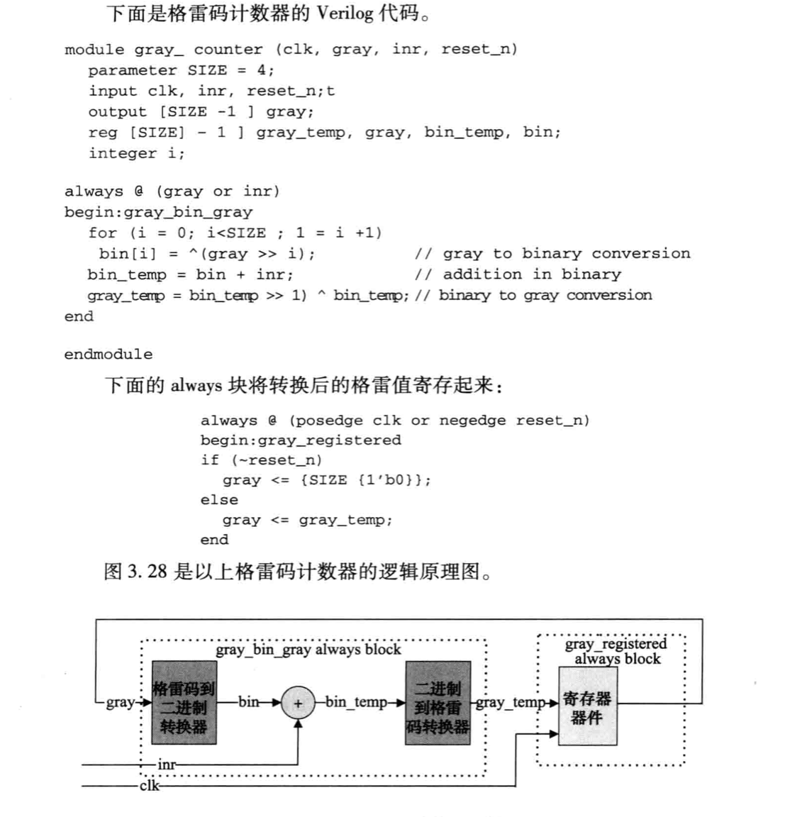
Design concept of gray code counter: Gray code to binary converter, adder, binary code to gray code converter, register for saving gray value
3. Corresponding module code segment
1) Top level module
//************Top level module*************************
`timescale 1 ns/ 1 ps
module asyn_fifo_top #(
	parameter DATA_WIDTH = 8,
	parameter ADDR_WIDTH = 4,
	parameter RAM_DEPTH = 16
)
(
	input 		              WCLK,
	input                         WRSTn,
	input                         RCLK,
	input                         RRSTn,
	input                         write,
	input                         read,
	input  [ DATA_WIDTH - 1 : 0 ] wdata,
	output [ DATA_WIDTH - 1 : 0 ] rdata,
	output                        full,
	output                        empty
);

wire [ ADDR_WIDTH : 0 ]    wpt;
wire [ ADDR_WIDTH : 0 ]    rpt;
wire [ ADDR_WIDTH : 0 ]    rp2_wpt;
wire [ ADDR_WIDTH : 0 ]    wp2_rpt;
wire [ ADDR_WIDTH - 1: 0 ] waddr;
wire [ ADDR_WIDTH - 1: 0 ] raddr;

double_ram#(.DATA_WIDTH(DATA_WIDTH),
			.ADDR_WIDTH(ADDR_WIDTH),
			.RAM_DEPTH(RAM_DEPTH))
	ram_module (.WCLK(WCLK),
	            .write(write),
				.waddr(waddr),
				.wdata(wdata),
				.raddr(raddr),
				.rdata(rdata));
r2w_sync #(.ADDR_WIDTH(ADDR_WIDTH))
	r2w_module (.WCLK(WCLK),
				.WRSTn(WRSTn),
				.rpt(rpt),
				.rp2_wpt(rp2_wpt));
w2r_sync #(.ADDR_WIDTH(ADDR_WIDTH))
	w2r_module (.RCLK(RCLK),
				.RRSTn(RRSTn),
				.wpt(wpt),
				.wp2_rpt(wp2_rpt));
full#(.ADDR_WIDTH(ADDR_WIDTH))
	full_module(.WCLK(WCLK),
				.WRSTn(WRSTn),
				.write(write),
				.rp2_wpt(rp2_wpt),
				.wpt(wpt),
				.waddr(waddr),
				.full(full));
empty #(.ADDR_WIDTH(ADDR_WIDTH))
	empty_module(.RCLK(RCLK),
				 .RRSTn(RRSTn),
				 .read(read),
				 .wp2_rpt(wp2_rpt),
				 .rpt(rpt),
				 .raddr(raddr),
				 .empty(empty));


endmodule
3.2 RAM module
//******************Dual interface RAM******************
module double_ram#(
	parameter DATA_WIDTH = 8,
	parameter ADDR_WIDTH = 4,
	parameter RAM_DEPTH = 16
)
(
	input                       WCLK,   //write clk
	input 					    write,  //write en
	input  [ ADDR_WIDTH - 1:0 ] waddr,  //write address from full.v
	input  [ DATA_WIDTH - 1:0 ] wdata,  //write data
	input  [ ADDR_WIDTH - 1:0 ] raddr,  //read address from empty.v
	output  [ DATA_WIDTH - 1:0 ] rdata   //read data
);

reg [ DATA_WIDTH - 1:0 ] RAM [ RAM_DEPTH - 1:0 ];  //double Port ram


always @ ( posedge WCLK )
begin
	if ( write == 1'b1 )
	begin
		RAM [ waddr ] <= wdata;
	end
	else
	begin
		RAM [ waddr ] <= RAM [ waddr ];
	end
end

assign rdata = RAM [ raddr ];

endmodule
3) Judge full logic module
//*****************Judge full logic****************
module full#(
	parameter ADDR_WIDTH = 4
)
(
	input                           WRSTn,
	input                           WCLK,
	input                           write,
	input      [ ADDR_WIDTH : 0 ]   rp2_wpt,
	output reg [ ADDR_WIDTH : 0 ]   wpt,
	output     [ ADDR_WIDTH - 1:0 ] waddr,
	output reg                      full
);

reg  [ ADDR_WIDTH :0 ] wbin;
wire [ ADDR_WIDTH :0 ] wbin_next;
wire [ ADDR_WIDTH :0 ] wgray_next;
wire                   full_reg;

always @ ( posedge WCLK or negedge WRSTn )
begin
	if (!WRSTn)
	begin
		wpt <= 0;
		wbin <= 0;
	end
	else
	begin
		wpt <= wgray_next;
		wbin <= wbin_next;
	end
end

assign wbin_next = ( !full ) ? ( wbin + write ) : wbin;
assign wgray_next = ( wbin_next >> 1 ) ^ wbin_next;
assign waddr = wbin [ ADDR_WIDTH - 1:0 ];


always @ ( posedge WCLK or negedge WRSTn )
begin
	if (!WRSTn)
	begin
		full <= 0;
	end
	else
	begin
		full <= full_reg;
	end
end

assign full_reg = ( wgray_next == { -rp2_wpt [ ADDR_WIDTH : ADDR_WIDTH - 1],rp2_wpt [ ADDR_WIDTH - 2:0]});

endmodule
4) Determine whether it is a null pointer
//********************Judge whether it is empty logic************
module empty#(
	parameter ADDR_WIDTH = 4
)
(
	input                           RRSTn,
	input                           RCLK,
	input                           read,
	input      [ ADDR_WIDTH : 0 ]   wp2_rpt,
	output reg [ ADDR_WIDTH : 0 ]   rpt,
	output reg [ ADDR_WIDTH - 1:0 ] raddr,
	output reg                      empty
);

reg  [ ADDR_WIDTH :0 ] rbin;
wire [ ADDR_WIDTH :0 ] rbin_next;
wire [ ADDR_WIDTH :0 ] rgray_next;
wire                   empty_reg;

always @ ( posedge RCLK or negedge RRSTn )
begin
	if (!RRSTn)
	begin
		rpt <= 0;
		rbin <= 0;
	end
	else
	begin
		rpt <= rgray_next;
		rbin <= rbin_next;
	end
end

assign rbin_next = ( !empty ) ? ( rbin + read ) : rbin;
assign rgray_next = ( rbin_next >> 1 ) ^ rbin_next;
//assign raddr = rbin [ ADDR_WIDTH - 1:0 ];

always @ ( posedge RCLK or negedge RRSTn )
begin
	if (read)
	begin
	   raddr <= rbin [ ADDR_WIDTH - 1:0 ];
	end

end

always @ ( posedge RCLK or negedge RRSTn )
begin
	if (!RRSTn)
	begin
		empty <= 0;
	end
	else
	begin
		empty <= empty_reg;
	end
end

assign empty_reg = ( rgray_next == wp2_rpt );

endmodule
5) Read write cross clock domain
//****************Read write cross clock domain****************
module r2w_sync#(
	parameter ADDR_WIDTH = 4
)
(
	input 						  WRSTn,    //write RSTn
	input 					      WCLK,     //write CLK
	input      [ ADDR_WIDTH : 0 ] rpt,      //output to write port gray
	output reg [ ADDR_WIDTH : 0 ] rp2_wpt   //D trigger sync with two levels,second level
);


reg [ ADDR_WIDTH : 0 ] rp1_wpt;         //frist level
//reg [ ADDR_WIDTH : 0 ] rp2_wpt;

always @ ( posedge WCLK or negedge WRSTn )
begin
	if ( !WRSTn )
	begin
		{ rp2_wpt,rp1_wpt } <= 0;
	end
	else
	begin
		{ rp2_wpt,rp1_wpt } <= { rp1_wpt,rpt };
	end
end

endmodule
6) Write read cross clock domain
/**Write to Read Sync module**/
module w2r_sync#(
	parameter ADDR_WIDTH = 4
)
(
	input 						  RRSTn,    //read RSTn
	input 						  RCLK,     //reaf CLK
	input      [ ADDR_WIDTH : 0 ] wpt,      //output to read port gray
	output reg [ ADDR_WIDTH : 0 ] wp2_rpt   //D trigger sync with two levels,second level
);

reg [ ADDR_WIDTH : 0 ] wp1_rpt;         //frist level
//reg [ ADDR_WIDTH : 0 ] wp2_rpt;

always @ ( posedge RCLK or negedge RRSTn )
begin
	if ( !RRSTn )
	begin
		{ wp2_rpt,wp1_rpt } <= 0;
	end
	else
	begin
		{ wp2_rpt,wp1_rpt } <= { wp1_rpt,wpt};
	end
end

endmodule
4.tb
`timescale 1 ns/ 1 ps
module asyn_fifo_tb();

parameter DATA_WIDTH = 8;

	reg                         WCLK;
	reg                         WRSTn;
	reg                         RCLK;
	reg                         RRSTn;
	reg                         write;
	reg                         read;
	reg  [ DATA_WIDTH - 1 : 0 ] wdata;
	wire [ DATA_WIDTH - 1 : 0 ] rdata;
	wire                        full;
	wire                        empty;
	//integer                     i = 0;

asyn_fifo_top asyn_fifo(.WCLK(WCLK),
						.WRSTn(WRSTn),
						.RCLK(RCLK),
						.RRSTn(RRSTn),
						.write(write),
						.read(read),
						.wdata(wdata),
						.rdata(rdata),
						.full(full),
						.empty(empty));
initial
begin
	WCLK <= 0;
	forever #100 WCLK = ~WCLK;
end

initial
begin
	RCLK <= 0;
	forever #200 RCLK = ~RCLK;
end

initial
begin
	WRSTn = 0;
	wdata = 0;
	#100 WRSTn = 1;
end

initial
begin
	RRSTn = 0;
	#100 RRSTn = 1;
	#10000;
	$finish();
end


always @ ( posedge WCLK or negedge WRSTn )
begin
	wdata <= wdata + 1'b1;
end

//always  @(posedge WCLK or negedge WRSTn)
//begin
//      if(WRSTn==1'b0)
//      begin
//         i <= 0;
//      end
//      else if(!full)
//      begin
//         i = i+1;
//      end
//      else begin
//         i <= i;
//      end
//end

//always @ (*)
//begin
//    if (!full)
//        wdata = i;
//    else
//        wdata = 0;
//end


always @ ( full or WRSTn )
begin
	if (!WRSTn)
	begin
		write <= 0;
	end
	else if (!full)
	begin
		write <= 1;
	end
	else
	begin
		write <= 0;
	end
end

always @ ( empty or RRSTn )
begin
	if (!RRSTn)
	begin
		read <= 0;

	end

	else if (!empty)
	begin
		read <= 1;
	end
	else
	begin
		read <= 0;
	end
end

        initial begin
            $fsdbDumpfile("jacky");
            $fsdbDumpvars;
            $vcdpluson;
        end


endmodule
2, Another design idea (from csdn:FPGA)
//asyn_fifo code
module asyn_fifo #(
    parameter data_width = 16;
    parameter data_depth = 8;
    parameter ram_depth = 256;
    )
    (
        input       rst_n,

        input                       wr_clk,         //Write clock domain signal
        input                        wr_en,
        input   [data_width-1:0]    data_in,
        output                      full,

        input                       rd_clk,         //Clock reading domain signal
        input                       rd_en,
        input   [data_width-1:0]    data_out,
        output                      empty,
    )

    reg [data_depth-1:0]            wr_adr;         //Defines the address of the read-write pointer
    reg [data_depth-1:0]            rd_adr;

    reg [data_depth:0]              wr_adr_ptr ;    //Defines the pointer used for comparison
    reg [data_depth:0]              rd_adr_ptr ;

    wire [data_depth:0]             wr_adr_gray;    //Convert the pointer used for comparison to gray code
    reg [data_depth:0]              wr_adr_gray1 ;  //Used in two shots
    reg [data_depth:0]              wr_adr_gray2 ;
    wire [data_depth:0]             rd_adr_gray;    //Convert the pointer used for comparison to gray code
    reg [data_depth:0]              rd_adr_gray1 ;  //Used in two shots
    reg [data_depth:0]              rd_adr_gray2 ;


    //*********************Data read / write module defined in dual port ram******************
    assign wr_adr  =  wr_adr_ptr[data_depth-1:0]    //Defines the relationship between the comparison pointer and the read / write pointer
    assign rd_adr  =  rd_adr_ptr[data_depth-1:0]

    integer i;                                      //Instantiate a RAM
    reg [data_width-1:0]  ram_fifo [data_depth-1:0] ;
        //Write in ram
    always @ (posedge wr_clk or negedge rst_n)
        begin
        if(!rst_n)
            begin                                   //Set all ram to zero
                for(i;i<ram_depth;i=i+1)
                    ram_fifo[i] <= 'd0;
            end
        else if (wr_en && ~full)
            ram_fifo[wr_adr] <= data_in;
        else
            ram_fifo[wr_adr] <= ram_fifo[wr_adr];
        end

        //Reading data in ram
    always @ (posedge rd_clk or rst_n)
        begin
        if (!rst_n)
            data_out <= 'd0;
        else if (rd_en && ~empty)
            data_out <= ram_fifo [rd_adr];
        else
            data_out <= 'd0;
         end
//**********After reading and writing, add 1 to the comparison pointer************
    always @ (posedge wr_clk or !rst_n)
        begin
            if (!rst_n)
                wr_adr_ptr <='b0;
            else if (wr_en && ~full)
                wr_adr_ptr <= wr_adr_ptr + 1'b1;
            else
                wr_adr_ptr <= wr_adr_ptr
        end
    always @ (posedge rd_clk or !rst_n)
        begin
            if (!rst_n)
                rd_adr_ptr <= 'b0;
            else if (rd_en && ~empty)
                rd_adr_ptr <= rd_adr_ptr + 1'b0;
            else
                rd_adr_ptr <= rd_adr_ptr
        end


 //**********************Convert comparison pointer to gray code*******************
    assign wr_adr_gray = (wr_adr_ptr >> 1)^ wr_adr_ptr;
    assign rd_adr_gray = (rd_adr_ptr >> 1) ^ rd_adr_ptr;

//*************************Compare the size of gray code************
   //When judging whether it is empty, judge whether the converted gray codes are equal in the time reading clock field
   //When judging whether it is full, compare the highest bits of gray code and the remaining bits in the write clock field

   //Make two beats of the comparison gray code under the corresponding clock to synchronize the clock domain
   always @ (posedge wr_clk or !rst_n)
        begin
        if (!rst_n)
            begin
                rd_adr_gray1 <= 'b0;
                rd_adr_gray2 <= 'b0;
            end
        else begin
            rd_adr_gray1 <= rd_adr_gray;
            rd_adr_gray2 <= rd_adr_gray1;
            end
        end
   always @ (posedge rd_clk or !rst_n)
        begin
        if (!rst_n)
            begin
                wr_adr_gray1 <= 'b0;
                wr_adr_gray2 <= 'b0;
            end
        else begin
            wr_adr_gray1 <= wr_adr_gray;
            wr_adr_gray2 <= wr_adr_gray1;
            end
        end

        //Judge empty and full
    assign empty = (rd_adr_gray2 == wr_adr_gray2) ? 1'b:1'b0;
    assign full = (rd_adr_gray2[data_depth : data_depth-1] != wr_adr_gray2[data_depth:data_depth-1]) && (wr_adr_gray2[data_depth-2:0] == rd_adr_gray2[data_depth-2:0])


endmodule
tb
//testbench for asynchronous fifo
`timescale 1ns/1ps

module asyn_fifo_tb;

    reg                 rst_n;

    reg                 wr_clk;
    reg                 wr_en;
    reg     [15:0]      data_in;
    wire                full;

    reg                 rd_clk;
    reg                 rd_en;
    reg     [15:0]      data_out;
    wire                empty;


    asyn_fifo asyn_fifo_inst
    (
        .rst_n      (rst_n),

        .wr_clk     (wr_clk),
        .wr_en      (wr_en),
        .data_in    (data_in),
        .full       (full),

        .rd_clk     (rd_clk),
        .rd_en       (rd_en),
        .data_out       (data_out),
        .empty      (empty)
    )

    //Define clock
    initial begin
        wr_clk = 0;
        forever #10 wr_clk = ~wr_clk;
    end

    initial begin
        rd_clk = 0 ;
        forever  #30 rd_clk = ~rd_clk;
    end

    // Define input data_in
    always @ (posedge wr_clk or negedge  rst_n)
        begin
            if (!rst_n)
                data_in <= 'd0;
            else if (wr_en)
                data_in <= data_in + 1'b1;
            else
                data_in <= data_in;
        end
    //Define other input signals

initial begin
    rst_n = 0;
    wr_en =0;
    rd_en = 0;
    #200
    rst_n = 1;
    wr_en = 1;
    #20000
    wr_en = 0;
    rd_en = 1;
    #20000
    rd_en = 0;

    $stop
end
endmodule