First raise a few questions:
1. What is OSERDES? What is the function of OSERDES? Use scenarios?
2. What is the structure of OSERDES? What ports are there? What are the port properties?
3.OSERDES parameter property description?
4. How do OSERDES bit extensions work?
5. What is the OSERDES timing, latency, 3-state control?
6. What to do with time series simulation? First the simulation result is shown, then the code is pasted.
Understanding the above questions will give you a clear idea of how OSERDES is used, followed by an explanation of OSERDES in the order of the above questions.
Note that this time OSERDES is used. A single OSERDES has only six parallel data input ports. Now there is OSERDESE2. A single OSERDESE2 has eight parallel data input ports.
1. What is OSERDES? What is the function of OSERDES? Use scenarios?
The full name of OSERDES is output parallel-to-serial logic resources, which is used to convert parallel data to serial data output. This IP is commonly used in transmitting video signals such as HDMI, LVDS, etc.
2. What is the structure of OSERDES? What ports are there? What are the port properties?
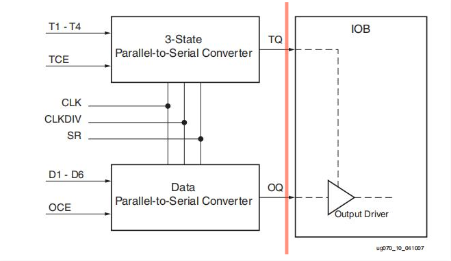
The OSERDES is briefly structured as the left half of the red line in the diagram. The ports can be divided into three types: three-state output control signal, clock control signal and parallel-to-serial conversion signal. The right half of the red line in the diagram is IOB, which is included in this article. Add Link Description As mentioned, you can archaeology.
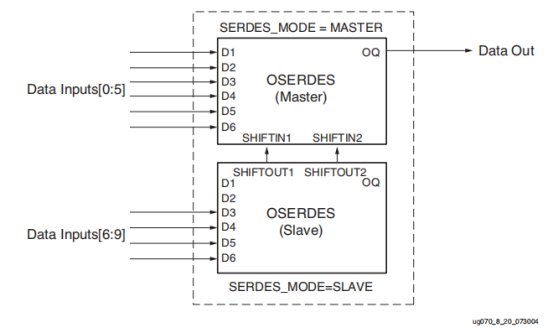
In fact, the detailed structure of OSERDES is as follows, unlike the figure above, two sets of ports have been added: SHIFTIN1/2, SHIFTOUT1/2. When the width of a single OSERDES cannot meet the same set of parallel data widths to be converted in parallel, two OSERDES need to be cascade d.
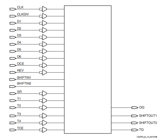
Port description;
CLKDIV: Slow clock, parallel data input clock
CLK: High Speed Clock, Serial Data Output Clock
D1-D6: Parallel data input
OQ: Parallel data output
OCE: Output clock enable
SR: Reset signal, highly effective
TI-T4: Three-state control parallel input
TCE: Three-state clock enable
TQ: Three-state control output
SHIFTOUT1/2: Output signal from OSERDES when the parallel data bit width exceeds the 6-bit conversion capacity of OSERDES
SHIFTIN1/2: Main OSERDES input signal when the parallel data bit width exceeds the 6-bit conversion capacity of OSERDES
REV: Inverse reset signal, assigned 0 when used
3.OSERDES parameter property description?
When using OSERDES, there are nine parameters that need to be assigned, mainly defining the operating mode and initial signal of OSERDES.
Parameter description:
DATE_RATE_OQ: "DDR" stands for OQ's output along both sides of the CLK, and "SDR" stands for OQ's output along the rising edge of the CLK. The default value is "DDR";
DATA_RATE_TQ:'DDR'stands for TQ's output along both sides of the CLK,'SDR' stands for TQ's output along the rise of the CLK, and'BUF'stands for three-state control as a buffer, with the default value of'DDR';
DATA_WIDTH: Parallel input data bit width, when DATE_RATE_OQ is "DDR", the value can be 4, 6, 8, 10; when DATE_RATE_OQ is "SDR", the value can be 2, 3, 4, 5, 6, 7, 8; the default value is 4;
SERDES_MODE: Used when the parallel data bit width exceeds the 6-bit conversion capability of OSERDES, the value can be "MASTER", "SLAVE", and the default value is "MASTER";
TRISTATE_WIDTH: Three-state control bit width, when DATE_RATE_TQ is "DDR", the value can be 2, 4; when DATE_RATE_TQ is "SDR" or "BUF", the value can only be 1, the default value is 4;
INIT_OQ: Defines the initial value of OQ;
INIT_TQ: Defines the initial value of TQ;
SRVAL_OQ: Defines the value of OQ at reset;
SRVAL_TQ: Defines the value of OQ at reset.
4. How to use OSERDES bit extension
When using OSERDES bit extension function, D1 and D2 from (SLAVE) OSERDES cannot be used, so OQ can only be converted in parallel at most 10:1. When DATE_RATE_OQ is "DDR", parallel data bit widths for parallel conversion can be 4, 6, 8, 10; DATE_RATE_OQ is "SDR"Parallel data bitwidths for parallel conversion can be 2, 3, 4, 5, 6, 7, 8.
At the same time, it should be noted that the signal at D1 end is transmitted first, then D2, D3...
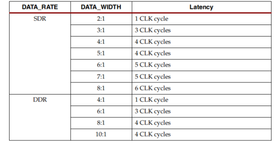
5.OSERDES timing specification, latency delay, 3-state control
OSERDES Latence is defined as the first bit along which the CLKDIV clock collects D1-D6 data to output at the OQ end. The delay depends on the parameters DATE_RATE_OQ and DATA_WIDTH in CLK time, as shown in the following table
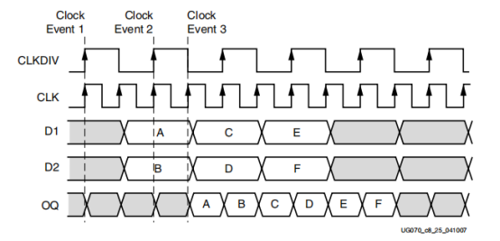
(1) The time sequence of OSERDES transmission in 2:1 SDR mode is as follows. It can be seen that D1, D2 data A and B are collected along the rising edge of Clock Event2, A is output from Clock Event3, and the two clock events are 1 CLK different
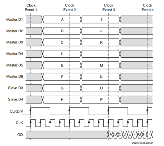
(2) Looking at the 8:1 DDR mode, you can see data A and B collected from Clock Event2 rising edge to D1 and D2, Clock Event3 starts to output A, and two clock events differ by 4 CLK s.
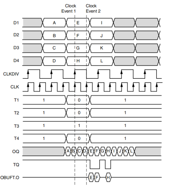
(3) DDR three-state control mode of 4:1, T3 is set at 1 in Clock Event2, resulting in no output of data G of D3 port. Three-state control mode is not used in video signal output at present, because it only makes output.
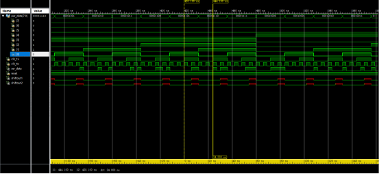
6.8:1 DDR mode simulation
In 8:1 DDR mode simulation, how OSERDES cascade to convert in parallel, this time the output of OQ is not controlled in three states, so T1-T4 is assigned to 0.
The module code is as follows:
module oserdes(
	input clk_1x,
	input clk_4x,
	input clk_4x_phase_shift,
	input reset,
	input [7:0] par_data,
	output ser_data,
    );

wire shiftout1,shiftout2;

OSERDES #(
			.DATA_RATE_OQ ("DDR"),    // "DDR" or "SDR"
			.DATA_RATE_TQ ("DDR"),    // "DDR", "SDR", or "BUF"
			.DATA_WIDTH   (8),        // DDR: 4,6,8, or 10
                                      // SDR or BUF: 2,3,4,5,6,7, or 8
			.INIT_OQ      (1'b0),     // INIT for Q1 register - '1' or '0'
			.INIT_TQ      (1'b0),     // INIT for Q2 register - '1' or '0'
			.SERDES_MODE  ("MASTER"), //"MASTER" or "SLAVE"
			.SRVAL_OQ     (1'b0),     // Define Q1 output value upon SR assertion - '1' or '0'
			.SRVAL_TQ     (1'b0),     // Define Q1 output value upon SR assertion - '1' or '0'
			.TRISTATE_WIDTH(2)        // Specify parallel to serial converter width
                                     // When DATA_RATE_TQ = DDR: 2 or 4
							         // When DATA_RATE_TQ = SDR or BUF: 1
)
U_OSERDES_MASTER (
			.OQ(ser_data),
			.SHIFTOUT1(),
			.SHIFTOUT2(),
			.TQ(),
			.CLK(clk_4x),
			.CLKDIV(clk_1x),
			.D1(par_data[0]),
			.D2(par_data[1]),
			.D3(par_data[2]),
			.D4(par_data[3]),
			.D5(par_data[4]),
			.D6(par_data[5]),
			.OCE(1'b1),
			.REV(1'b0),
			.SHIFTIN1(shiftout1),
			.SHIFTIN2(shiftout2),
			.SR(~reset),
			.T1(1'b0),
			.T2(1'b0),
			.T3(1'b0),
			.T4(1'b0),
			.TCE(1'b0)
);

	OSERDES #(
			.DATA_RATE_OQ ("DDR"),    // "DDR" or "SDR"
			.DATA_RATE_TQ ("DDR"),    // "DDR", "SDR", or "BUF"
			.DATA_WIDTH   (8),        // DDR: 4,6,8, or 10
                                      // SDR or BUF: 2,3,4,5,6,7, or 8
			.INIT_OQ      (1'b0),     // INIT for Q1 register - '1' or '0'
			.INIT_TQ      (1'b0),     // INIT for Q2 register - '1' or '0'
			.SERDES_MODE  ("SLAVE"), //"MASTER" or "SLAVE"
			.SRVAL_OQ     (1'b0),     // Define Q1 output value upon SR assertion - '1' or '0'
			.SRVAL_TQ     (1'b0),     // Define Q1 output value upon SR assertion - '1' or '0'
			.TRISTATE_WIDTH(2)        // Specify parallel to serial converter width
                                     // When DATA_RATE_TQ = DDR: 2 or 4
							         // When DATA_RATE_TQ = SDR or BUF: 1
)
U_OSERDES_SLAVE (
			.OQ(),
			.SHIFTOUT1(shiftout1), //MASTER OSERDES SHIFTIN1
			.SHIFTOUT2(shiftout2), //MASTER OSERDES SHIFTIN2
			.TQ(),
			.CLK(clk_4x),
			.CLKDIV(clk_1x),
			.D1(),
			.D2(),
			.D3(par_data[6]),
			.D4(par_data[7]),
			.D5(),
			.D6(),
			.OCE(1'b1),
			.REV(1'b0),
			.SHIFTIN1(),
			.SHIFTIN2(),
			.SR(~reset),
			.T1(1'b0),
			.T2(1'b0),
			.T3(1'b0),
			.T4(1'b0),
			.TCE(1'b0)
);


endmodule
The simulation test code is as follows:
module tb_oserdes;

	// Inputs
	reg clk_1x;
	reg clk_4x;
	reg clk_4x_phase_shift;
	reg reset;
	reg [7:0] par_data;

	// Outputs
	wire ser_data;
	wire ser_data_p;
	wire ser_data_n;

	reg clk_1x_phase_shift;

	// Instantiate the Unit Under Test (UUT)
	oserdes uut (
		.clk_1x(clk_1x),
		.clk_4x(clk_4x),
		.clk_4x_phase_shift(clk_4x_phase_shift),
		.reset(reset),
		.par_data(par_data),
		.ser_data(ser_data),
		.ser_data_p(ser_data_p),
		.ser_data_n(ser_data_n)
	);

	initial begin
		// Initialize Inputs
		clk_1x = 0;
		clk_4x = 1;
		clk_4x_phase_shift = 0;
		reset = 0;
		par_data = 0;
		clk_1x_phase_shift = 1;

		// Wait 100 ns for global reset to finish
		#100;
		reset =1;
	end


		// Add stimulus here
		always #12 clk_1x = ~clk_1x;
		always #3  clk_4x = ~clk_4x;
		always #12 clk_1x_phase_shift = ~clk_1x_phase_shift;

		always @(posedge clk_1x_phase_shift or negedge reset)
		begin
			if(!reset)
				par_data <=8'b0;
			else
				par_data <= par_data + 1'b1;
		end


endmodule
The simulation results show that the delay is 4 CLK, which matches the latency table above.

7. Some Reflections on Extending
(1) OSERDES is generally a high-speed signal, and high-speed signal usually uses differential output to ensure the quality of the signal, while an I/O tile only has two OSERDES, how do MASTER and SLAVE allocate P/N pins when OSERDES is cascaded?
(2) Can DIFF_HSTL and DIFF_SSTL use non-extended functions, and why?