In the last article, I mainly talked about the realization of odd frequency division. This article explains how to design N+0.5 frequency divider. This article takes 5.5 frequency division as an example to illustrate. For N+0.5 frequency divider, there is no way to achieve a real duty ratio of 50%, so we can achieve a duty ratio of 1/(N+0.5) frequency divider, that is, to achieve a high level in 0.5 cycles.
First of all, a design idea: through the operation of two frequency division clocks. The duty cycle of two frequency division clocks is (N+1)/(2*N+1). For a 5.5 frequency division circuit, the duty cycle is 6/11. However, one of the two frequency division clocks is triggered based on the rising edge of the clock and the other is triggered based on the falling edge of the clock, and the initial value of the clock is opposite, so that the circuit with 5.5 frequency division can be obtained by comparing the two clock phases.
The code for implementation is as follows:
module half_div #(parameter N = 5)(
input clk_in,
input rst,
output clk_out);
reg [3:0] cnt1;
reg [3:0] cnt2;
reg div1;
reg div2;
always@(posedge clk_in or negedge rst)
begin
if(!rst)
begin
cnt1<=3'b0;
div1 <= 0;
end
else
begin
cnt1 <= cnt1 + 1'b1;
if(cnt1 == 2*N)
begin
cnt1 <= 0;
end
else if(cnt1 == N+1|| cnt1 == 0)
begin
div1 = ~div1;
end
end
end
always@(negedge clk_in or negedge rst)
begin
if(!rst)
begin
cnt2 <= 3'b0;
div2 <= 1'b1;
end
else
begin
cnt2 <= cnt2 + 1;
if(cnt2 == 2*N)
begin
cnt2 <= 0;
end
else if(cnt2 == N+1||cnt2 == 1)
begin
div2 = ~div2;
end
end
end
assign clk_out = div1 & div2;
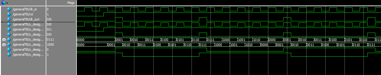
endmoduleThe simulation results are as follows:
When designing other N+0.5 frequency dividers, only the corresponding N can be replaced.
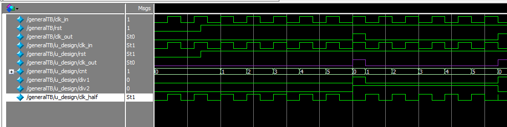
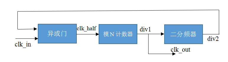
The second design idea is based on the universal half-integer frequency divider. Its design idea is to count N from 0 and output 1 when counting N. But in order to achieve N+0.5 cycles, the output 1 lasts half a cycle. In this case, the falling edge of the input clock needs to be changed into the rising edge, so that the output half-cycle length can be realized. 1. The rising edge of the input clock is changed into the falling edge by XOR of the output and input clocks of the two-frequency division.
Design schematic diagram:
Design code:
module half_div #(parameter N = 5)(
input clk_in,
input rst,
input clk_out);

reg [3:0] cnt;
reg div1;
reg div2;
wire clk_half;

assign clk_half = clk_in ^ div2;

always@(posedge clk_half or negedge rst)
begin
  if(!rst)
  begin
    cnt <= 0;
	div1 <= 0;
  end
  else if(cnt == N)
  begin
    cnt <= 0;
	div1 <= 1;
  end
  else
  begin
   cnt <= cnt + 1;
   div1 <= 0;
  end
end

always@(posedge div1 or negedge rst)
begin
  if(!rst)
     div2 <= 0;
  else div2 = ~div2;
end
assign clk_out = div1;

endmodule
The simulation output: