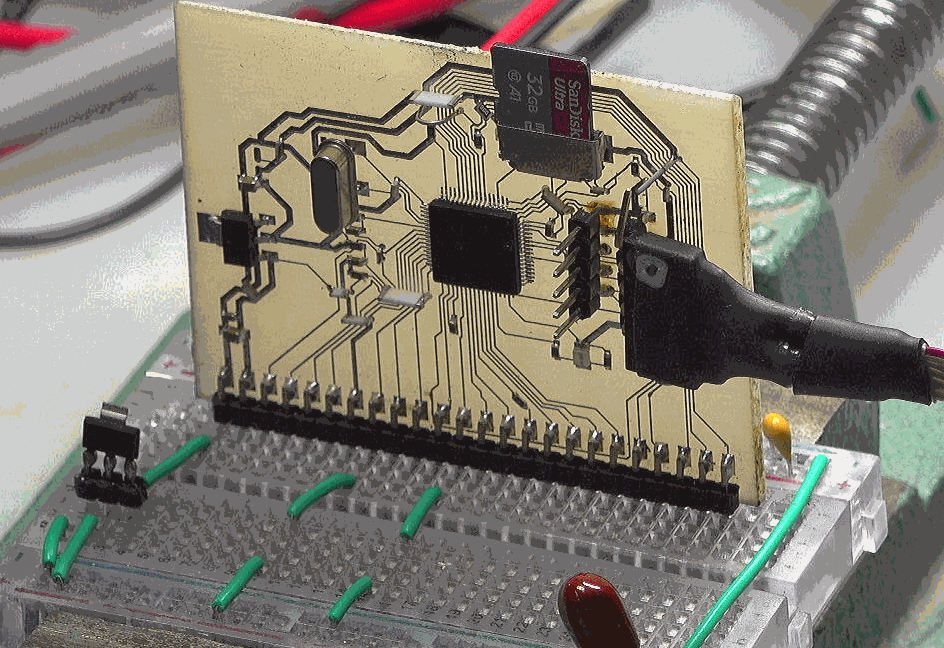
Introduction: Through the array mem in micropthon, the internal analog comparator of MM32F3277 is preliminarily tested to verify its most basic setting and working relationship. During the test, problems in the data manual and corresponding internal functions of MM32F3277 were also found: wrong description of COMP Control Register Offset and how to select the output port of the comparator.
Key words: MM32F3277, mem, COMP
§ 01 mem operation COMP
1, mem array
there is a group of arrays in micropthon that can directly access the memory of MCU. These arrays are:
- mem32
- mem16
- mem8
they access the RAM space of MCU through 4 bytes, 2 bytes and 1 byte respectively. Using them, you can access the ram inside MCU in the mode of list. The address parameter addr in mem32[addr] must be an integer multiple of 4, and the address parameter of mem16 must be an integer multiple of 2. mem8 has no limit.
1. mem array function
in the early stage, access to some module registers in microphoton was completed through mem numbers.
- Accessing module registers in microphoton through mem function
- Mm32f3277 micro Python mem function for MCU memory access
experiments show that using mem to complete memory operations can speed up the running speed to a certain extent, but the speed improvement is not obvious.
however, for the functions not supported in the micro Python kernel, the module operation inside the MCU can be completed through mem array access. For example, for the direct operation of CRC, UART and GPIO.
next, directly access the COMP module of the analog comparator inside MM32F3277.
2. COMP module
(1) COMP clock
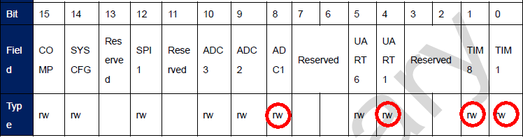
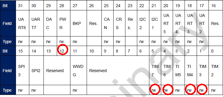
the MM32F3277 has two analog comparators, Comp1 and Comp2, which are mounted on the internal APB2.
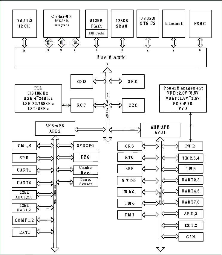
input clock of COMP and APB2_CLK synchronization. Before using the comparator, enable the clock enable control bit in the RCC controller. Configure the software reset request in the RCC controller to perform the software reset operation.
/// @brief RCC Base Address Definition
#define RCC_BASE (AHBPERIPH_BASE + 0x1000) ///< Base Address: 0x40021000
/// @brief RCC Register Structure Definition
typedef struct {
__IO u32 CR; ///< Control Register offset: 0x00
__IO u32 CFGR; ///< Configuration Register offset: 0x04
__IO u32 CIR; ///< Clock Interrupt Register offset: 0x08
__IO u32 AHB3RSTR; ///< Advanced High Performance Bus 3 Reset Register offset: 0x0C
__IO u32 AHB2RSTR; ///< Advanced High Performance Bus 2 Reset Register offset: 0x10
__IO u32 AHBRSTR; ///< Advanced High Performance Bus 1 Reset Register offset: 0x14
__IO u32 APB2RSTR; ///< Advanced Peripheral Bus 2 Reset Register offset: 0x18
__IO u32 APB1RSTR; ///< Advanced Peripheral Bus 1 Reset Register offset: 0x1C
__IO u32 AHB3ENR; ///< Advanced High Performance Bus 3 Enable Register offset: 0x20
__IO u32 AHB2ENR; ///< Advanced High Performance Bus 2 Enable Register offset: 0x24
union {
__IO u32 AHBENR; ///< Advanced High Performance Bus 1 Enable Register offset: 0x28
__IO u32 AHB1ENR;
};
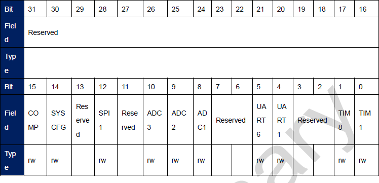
__IO u32 APB2ENR; ///< Advanced Peripheral Bus 2 Enable Register offset: 0x2C
__IO u32 APB1ENR; ///< Advanced Peripheral Bus 1 Enable Register offset: 0x30
__IO u32 BDCR; ///< Backup Domain Control Register offset: 0x34
__IO u32 CSR; ///< Control Status Register offset: 0x38
__IO u32 SYSCFGR; ///< System Configuration Register offset: 0x3C
__IO u32 CFGR2; ///< System Configuration Register offset: 0x40
__IO u32 ICSCR; ///< Internal clock source calibration register offset: 0x44
__IO u32 PLLCFGR; ///< PLL configures registers offset: 0x48
u32 Reserved1[13]; ///< Reserved space
__IO u32 HSIDLY; ///< HSI delay register offset: 0x80
__IO u32 HSEDLY; ///< HSE delay register offset: 0x84
__IO u32 PLLDLY; ///< PLL delay register offset: 0x88
} RCC_TypeDef;
for APB2 in RCC, the address is:
RCC_BASE = 0x40021000
APB2ENR = 11*4
APB1ENR = 12*4
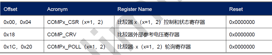
(2)COMP BASE
/// @brief COMP Base Address Definition

#define COMP_BASE                       (APB2PERIPH_BASE + 0x4000)              ///< Base Address: 0x40014000


/// @brief Comparators Register Structure Definition

typedef struct {

    __IO u32 RESERVED1;                                                         ///<                                                offset: 0x00
    __IO u32 RESERVED2;                                                         ///<                                                offset: 0x04
    __IO u32 RESERVED3;                                                         ///<                                                offset: 0x08
    union {
        __IO u32 CSR1;                                                          ///< COMP1 Control Status Register                  offset: 0x0C
        __IO u32 COMP1_CSR;
    };
    union {
        __IO u32 CSR2;                                                          ///< COMP2 Control Status Register                  offset: 0x10
        __IO u32 COMP2_CSR;
    };
    __IO u32 RESERVED4;                                                         ///<                                                offset: 0x14
    union {
        __IO u32 CRV;                                                           ///< COMP external reference voltage register       offset: 0x18
        __IO u32 COMP_CRV;
    };
    union {
        __IO u32 POLL1;                                                         ///< COMP1 polling register                         offset: 0x1C
        __IO u32 COMP1_POLL;
    };
    union {
        __IO u32 POLL2;                                                         ///< COMP2 polling register                         offset: 0x20
        __IO u32 COMP2_POLL;
    };
} COMP_TypeDef;
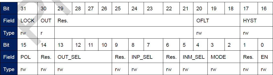
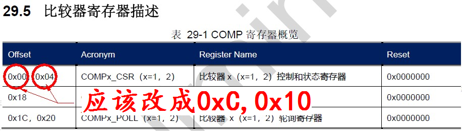
note that in the above structure definition, the address of the comparator is different from the definition in the data manual!
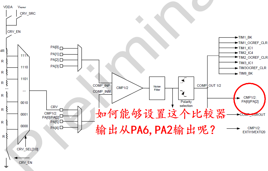
(3) Functional block diagram
the following is the function block diagram of COMP1,2 in the MM32F3277 data manual.
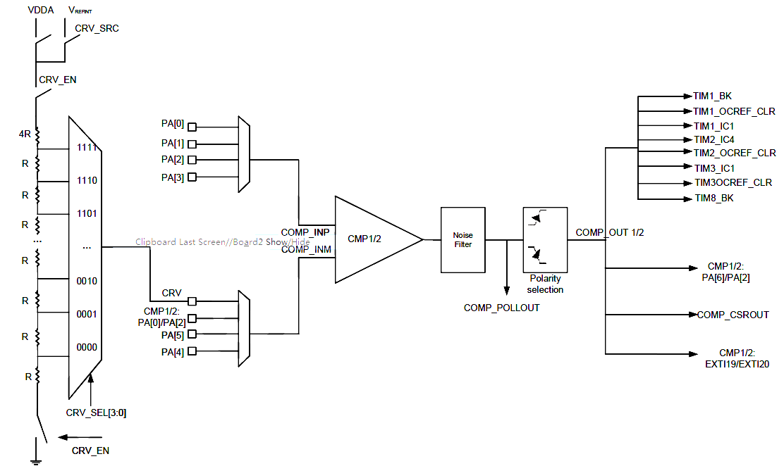
it can be seen from the system block diagram that the INP of two analog comparators can be selected: PA[0], PA[1],PA[2],PA[3]
INM can input: CRV, PA[0]/PA[2], PA[5], PA[4]
2, Preliminary test
1. Clock operation
(1) Basic operation
from machine                import Pin,mem32
import utime
from micropython            import const

RCC_BASE    = const(0x40021000)
APB2ENR     = const(RCC_BASE+11*4)
APB1ENR     = const(RCC_BASE+12*4)

print('%08x'%mem32[APB2ENR])
print('%08x'%mem32[APB1ENR])
output result:
00000113
10000036
(2) Add UART2
an initialization for UART2 is added.
uart2 = UART(1, 115200)

print('%08x'%mem32[APB2ENR])
print('%08x'%mem32[APB1ENR])
program running results:
00000113
10020036
you can see that there are more corresponding UART2 initialization in the corresponding APB1.
(3) COMP1,2 allowed
RCC_BASE = const(0x40021000)
APB2ENR = const(RCC_BASE+11*4)
APB1ENR = const(RCC_BASE+12*4)
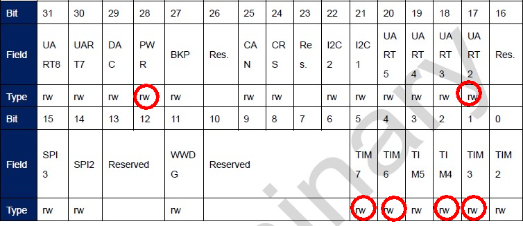
mem32[APB2ENR] |= 0x8000
print('%08x'%mem32[APB2ENR])
print('%08x'%mem32[APB1ENR])
the results of operation are:
00008113
10020036
at this time, the corresponding COMP1,2 clock is allowed.
2. COMP register
(1) Read initial value
COMP_BASE = const(0x40014000)
COMP_CSR1 = const(COMP_BASE+0xc)
COMP_CSR2 = const(COMP_BASE+0x10)
COMP_CRV  = const(COMP_BASE+0x18)
COMP_POLL1 = const(COMP_BASE+0x1c)
COMP_POLL2 = const(COMP_BASE+0x20)

print('%08x'%mem32[COMP_CSR1])
print('%08x'%mem32[COMP_CSR2])
print('%08x'%mem32[COMP_CRV])
print('%08x'%mem32[COMP_POLL1])
print('%08x'%mem32[COMP_POLL2])
initial value:
00000000
00000000
00000000
00000000
00000000
(2) Enable COMP12
mem32[COMP_CSR1] |= 0x1
mem32[COMP_CSR2] |= 0x1
print('%08x'%mem32[COMP_CSR1])
print('%08x'%mem32[COMP_CSR2])
00000001
40000001
strangely, the settings of the two comparators are the same, but their OUT is inconsistent!
3. Set external voltage
(1) Set PA0 and PA4 to high and low levels respectively
output result:
40000001
40000001
(2) Set PA0 and PA4 to low and high levels respectively
output result:
00000001
00000001
the result reflected by the above OUT position in CSR is the result of external voltage change.
4. COMP output signal
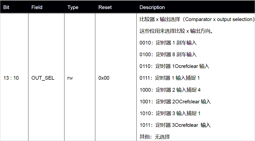
through the internal structure of COMP, you can see that the output pin of OUT corresponds to PA[6]/PA[2]. However, the CSR controls OUT_SEL does not give the option to output to PA6 and pa2.
the following can only be tested by software.
for OUT through software_ The SEL setting is from 0 to 15, but there is no change in the corresponding PA6. No matter how the detection OUT declares:
out = Pin('PA6', Pin.AF_PUSHPULL)
3, Test CRV
set the input of the INM of the comparator to CRV, and the negative input of the comparator can be set to the internal reference voltage.
1. Register setting
mem32[COMP_CSR1] = (0x1 | 0x30)
mem32[COMP_CSR2] = (0x1 | 0x30)
mem32[COMP_CRV]  = (0x3F)
print('%08x'%mem32[COMP_CSR1])
print('%08x'%mem32[COMP_CSR2])
print('%08x'%mem32[COMP_CRV])
corresponding at this time:
- SRV-SRC: 1: corresponding to VDDA;
- CRV_EN: 1: enables the reference voltage.
if PA0 is set to 3.3V, the output is:
40000031
40000031
0000003f
if PA0 is set to 0V, the output is:
00000031
00000031
0000003f
this indicates that the comparator works normally.
2. Set PA0 bit 1/2 VCC
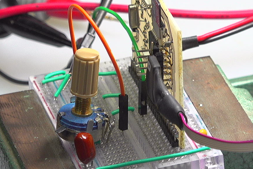
set PA0 to 1.66V through potentiometer.
(1) Set CRV
set CRV from 0 to 0xf successively, and read OUT the value of OUT respectively.
for i in range(16):
    mem32[COMP_CRV] = 0x30 | i
    print('%d, %08x'%(i, mem32[COMP_CSR1]))
(2) Test results
0, 40000031
1, 40000031
2, 40000031
3, 40000031
4, 40000031
5, 40000031
6, 40000031
7, 40000031
8, 40000031
9, 00000031
10, 00000031
11, 00000031
12, 00000031
13, 00000031
14, 00000031
15, 00000031
it can be seen that at this time, the corresponding CRV changes between 8 and 9. At this time, they correspond to:
- 9/20×VDDA = 1.484V
- 10/20×VDDA=1.65V
this is indeed near the medium potential.
3. Set PA0 to 2V
use potentiometer to set PA0 bit 2V. Run the above program and the output is:
0, 40000031
1, 40000031
2, 40000031
3, 40000031
4, 40000031
5, 40000031
6, 40000031
7, 40000031
8, 40000031
9, 40000031
10, 40000031
11, 00000031
12, 00000031
13, 00000031
14, 00000031
15, 00000031
※ general ※ conclusion ※
the analog comparator inside MM32F3277 is preliminarily tested through the array mem in micropthon to verify its most basic setting and working relationship.
during the test, problems in the data manual and corresponding internal functions of MM32F3277 were also found: wrong description of Register Offset and how to select the output port of the comparator.
1, Existing problems
1. Comparator offset
in the comparator register description in data manual 29.5, the Offset description of CSR is wrong.
2. Comparator output
in the manual, the outputs of the comparator are PA6 and pa2, but how to set them. This output signal cannot be tested at this time.
■ experimental procedure
#!/usr/local/bin/python
# -*- coding: gbk -*-
#============================================================
# TEST1.PY                     -- by Dr. ZhuoQing 2021-12-05
#
# Note:
#============================================================

from machine                import Pin,mem32,UART
import utime
from micropython            import const

#------------------------------------------------------------
led = Pin('PB2', Pin.OUT_PUSHPULL)
out1 = Pin('PA6', Pin.AF_PUSHPULL)
out1 = Pin('PA2', Pin.AF_PUSHPULL)

#------------------------------------------------------------
RCC_BASE    = const(0x40021000)
APB2ENR     = const(RCC_BASE+11*4)
APB1ENR     = const(RCC_BASE+12*4)

mem32[APB2ENR] |= 0x8000

#print('%08x'%mem32[APB2ENR])
#print('%08x'%mem32[APB1ENR])


#------------------------------------------------------------

COMP_BASE = const(0x40014000)
COMP_CSR1 = const(COMP_BASE+0xc)
COMP_CSR2 = const(COMP_BASE+0x10)
COMP_CRV  = const(COMP_BASE+0x18)
COMP_POLL1 = const(COMP_BASE+0x1c)
COMP_POLL2 = const(COMP_BASE+0x20)

#print('%08x'%mem32[COMP_CSR1])
#print('%08x'%mem32[COMP_CSR2])
#print('%08x'%mem32[COMP_CRV])
#print('%08x'%mem32[COMP_POLL1])
#print('%08x'%mem32[COMP_POLL2])

#------------------------------------------------------------
mem32[COMP_CSR1] = (0x1 | 0x30)
mem32[COMP_CSR2] = (0x1 | 0x30)
mem32[COMP_CRV]  = (0x3F)
#print('%08x'%mem32[COMP_CSR1])
#print('%08x'%mem32[COMP_CSR2])
#print('%08x'%mem32[COMP_CRV])

#------------------------------------------------------------
for i in range(16):
    mem32[COMP_CRV] = 0x30 | i
    print('%d, %08x'%(i, mem32[COMP_CSR1]))


while True:

    led.high()
    utime.sleep_ms(50)
    led.low()
    utime.sleep_ms(50)


#------------------------------------------------------------
#        END OF FILE : TEST1.PY
#============================================================
■ links to relevant literature:
- Accessing module registers in microphoton through mem function
- Mm32f3277 micro Python mem function for MCU memory access
● relevant chart links:
- Figure 1.1.1 COMP1,2 clock
- Figure 1.1.2 COMP1, 2 enable in apb2
- Figure 1.1.3 register address on Data Book
- Figure 1.1.4 function block diagram of comp1,2
- Figure 1.2.1 allowable position of apb2 clock
- Figure 1.2.2 APB1 clock allowable bit
- Figure 1.2.3 allowable position of apb1 clock
- Figure 1.2.4 control register
- Figure 1.2.5 PA0
- Figure 1.2.6 output selection control
- Figure 1.3.1 set PA0 to 1.66V using potentiometer
- Figure 2.1.2 data manual description error
- Figure 2.1.3 how to set the output of the comparator to PA6 and pa2