Record the pits and Bug solutions encountered in debugging on the Xilinx-Ego1, and Vivado's code-writing skills for developing the GA, so as to leave a background for future review. The whole article uses the development idea of single-chip computer to develop the field-bus, only to help readers get started quickly, and the development language is Verilog, which is the most commonly used.
For details on how to create a project using Vivado, see the Ego1 documentation for instructions on how to use Vivado, which is available on the website of the following elements: EGO1 (e-elements.com)
Click on the resource, register your mailbox, download the package, there are many routines:

source or ready-made project see 3c-EGo1 Configuration Experiment vivado2017.2_ Sorce and project folders in v1.2 folder

After learning the basic operation, teach you how to write code, first have a macro understanding of the whole code:
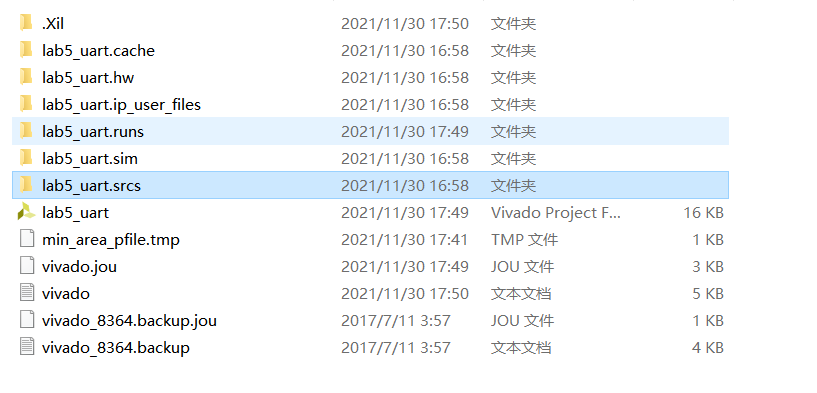
This is a folder of the project with lab5_ The code in the uart.srcs folder is written or created by you. The rest is generated automatically by vivado when you synthesize the simulation. The code is divided into two parts: a constraint file (.xdc) and a source file (.v)
Explain my understanding of Vivado's programming of a field bus project:
Source File (.v) File writing logic is layered (top and module layers), the driver code of the hardware you need to use is designed as a module, which has input and output. For example, if I want a digital tube to light up at a certain frequency, I need a timer, I need a clock as input, and of course, if you want to reset, I can also design a key. (rst) as input, then the output is 8 segments of the digital tube (8 LED s) , after designing the input and output, your logic is written, that is, when you let the digital tube light up, such as when I turn the digital tube on once in 1s and when it goes out again in 1s, you write the corresponding logic. Of course, you need to write the logic using the relevant grammar, grammar, novice bird tutorials and verilog language tutorials; then you need to define a top layer to input and transfer all your modules This module is instantiated (equivalent to the footer initialization of a single chip computer). Top layer is written when you design two or more modules, so that you can also look more convenient. All input and output of the system are in top layer, which is also convenient for you to view.
Constraint file is equivalent to pin definition when single chip computer is used. This is to constrain the input and output designed in top file of your source file to the related pin. Although you can not see pin in input and output such as clock and digital tube, you can understand that the logic of using the hardware driver based on the GA is: you design input and output, and then you will They are constrained to the relevant hardware or pin, which then goes to the hardware.
So my project is about Ego1's Trailer car. All the hardware driver codes are written by ego1 and he has the following functions:
Basic functions: can control DC encoder motor and rudder rotation with Ego1 output PWM wave, can read the track feedback signal of infrared track module with Ego1, can capture and collect encoder signal with Ego1 input to realize motor speed measurement, can output specific frequency square wave to drive passive buzzer to play music, and can display vehicle speed with Ego1 digital tube.
Ultimate function: After the car is powered on, it can automatically track while playing car music on the track.


System Hardware Configuration Design
(According to the requirements of the experiment, the system hardware configuration of the platform is discussed, including hardware selection, hardware matching, network connection and parameter configuration, etc.)
(1) Controller: Xilinx-Ego1 (GA)

(2) Actuator: Helicopter

(3) Executive element: encoder motor

(4) Actuator: Passive buzzer

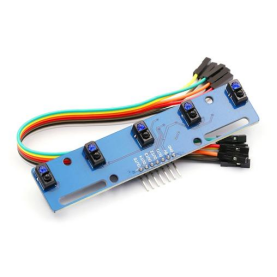
(5) Measuring element: Track module (5-way infrared sensor)
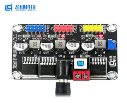
(6) Motor drive: tb6612fng

(7) Power amplifier unit: L298N
(8) Voltage regulator module:
The code for the rudder and motor modules is shown below: (Write together because they are all PWM)
Clock main frequency: clk constrained to P17, whether 50MHz or 100MHz I forgot
`timescale 1ns / 1ps

module  pwm_cont(
				clk,
				sw7,
				rst_n,
				da_in,
				pwm_out,
				pwm_outz,
				hw_in,
				djfz1,
				djfz2,
				djfy1,
				djfy2,
				pwm_outy
);

input					clk;
input					rst_n;
input					sw7;
input   [6:0]   	da_in;

output	reg		djfz1;
output	reg		djfz2;
output	reg		djfy1;
output	reg		djfy2;

output	reg		pwm_out;
output	reg		pwm_outz;
output	reg		pwm_outy;
input   [4:0]   	hw_in;
parameter          s=1000_000,//20ms-----min:s4 (left) max:s7 (right) middle: s1

                    s7=190_000,//4ms - Right Full
                    //s6=190_000,//3.5ms----270
                    s5=185_000,//3ms----225
					s0=175_000,//2.5ms - Right
					s1=150_000,//2ms - middle
					s2=125_000,//1.5ms----90
					s3=95_000,//1ms-----45 100_000
					s4=80_000;//0.5ms - 0 left full

reg	[31:0]   cnt_r;
reg	[31:0]	cnt;

reg	[31:0]   cnt_r1;
reg	[31:0]	cnt1;
reg biaoqian;
reg wr_reg,wr_up,wr_down;


always@(posedge clk or posedge rst_n)    begin
	if(rst_n)
	begin
	    wr_reg		<=		1'b0;
		wr_up		<=		1'b0;
		wr_down		<=		1'b0;
		cnt_r1 <= s1;
    end
	else
		begin
		wr_reg		<=		sw7;
		wr_up		<=		sw7&(~wr_reg);//sw1 Rise Edge Detection, Select Trace Mode
		wr_down		<=		~sw7&wr_reg;
		if(wr_up)
		biaoqian=1;
		if(wr_down)
		biaoqian=0;

		if(biaoqian==1)
		begin
		  djfz1=0;
		  djfz2=1;
		  djfy1=0;
		  djfy2=1;
			case(hw_in)
			    5'b00000:
			    begin
			    //Cnt_ R1 <= s1; // Middle
			    biaoqian<=0;
			    end
			    //5'b11111: cnt_ R1 <= s1; // Middle

			    5'b11000: cnt_r1 <= s7;//Turn right s7 full
			    5'b11110: cnt_r1 <= s7;//Turn right s7 full
			    5'b11100: cnt_r1 <= s5;//Turn left
			    5'b11101: cnt_r1 <= s0;//Turn left
			    5'b11001: cnt_r1 <= s1;//Middle
			    5'b11011: cnt_r1 <= s1;//Middle
			    5'b10011: cnt_r1 <= s1;//Middle
			    5'b10111: cnt_r1 <= s2;//Turn Right
			    5'b00111: cnt_r1 <= s3;//Turn Right
			    5'b01111: cnt_r1 <= s4;//Turn left s4 full
			    5'b00011: cnt_r1 <= s4;//Turn Right

			endcase
		end
		if(!biaoqian)
		begin
		  djfz1=0;
		  djfz2=0;
		  djfy1=0;
		  djfy2=0;
		end
		end
end

//Speed Selection
always@(posedge clk or posedge rst_n)begin
	if(rst_n)
	    begin
		cnt_r <= 31'd0;
		end
	else
		begin
//			case(da_in)//speed selection
//			    7'b0000001: cnt_r <= s/20;//90
//				//8'b00000011: cnt_r <= s4;//0
//				7'b0000010: cnt_r <= s/15;//45
//				7'b0000100: cnt_r <= s/10;//90
//				7'b0001000: cnt_r <= s/8;//135
//				7'b0010000: cnt_r <= s/4;//180
//				7'b0100000: cnt_r <= s/2;//225
//				7'b1000000: cnt_ R <= s; // Full speed
				case(hw_in)
				5'b11000: cnt_r <= s/8;//Turn right s7 full
			    5'b11110: cnt_r <= s/7;//Turn right s7 full
			    5'b11100: cnt_r <= s/7;//Turn left
			    5'b11101: cnt_r <= s/7;//Turn left
			    5'b11001: cnt_r <= s/5;//Middle
			    5'b11011: cnt_r <= s/5;//Middle
			    5'b11111: cnt_r <= s/5;//Middle
			    5'b10011: cnt_r <= s/5;//Middle
			    5'b10111: cnt_r <= s/7;//Turn Right
			    5'b00111: cnt_r <= s/7;//Turn Right
			    5'b01111: cnt_r <= s/7;//Turn left s4 full
			    5'b00011: cnt_r <= s/7;//Turn Right
			    5'b00000: cnt_r <= 0;//Stop it
				default: cnt_r <= s/8;//Stop it
			endcase
		end
end

always@(posedge clk or negedge rst_n)begin
	if(rst_n)
	begin
		cnt <= 31'd0;
		cnt1 <= 31'd0;
	end
	else if(cnt >= s)
	begin
		cnt <= 31'd0;
		cnt1 <= 31'd0;
	end
	else
	begin
		cnt <= cnt + 1'b1;
		cnt1 <= cnt1 + 1'b1;
	end
end

always@(posedge clk or negedge rst_n)begin
	if(rst_n)
	begin
		pwm_outz <= 1'b0;
		pwm_outy <= 1'b0;
    end
	else if(cnt <= cnt_r)
	begin
		pwm_outz <= 1'b1;
		pwm_outy <= 1'b1;
		if(wr_down)
	    begin
		  pwm_outz <= 1'b0;
		  pwm_outy <= 1'b0;
		end
	end
	else
	begin
		pwm_outz <= 1'b0;
		pwm_outy <= 1'b0;
	end
end

always@(posedge clk or negedge rst_n)begin
	if(rst_n)
	begin
	    //Pwm_ Out<= s1; // Middle
		pwm_out <= 1'b0;
    end
	else if(cnt1 <= cnt_r1)
	begin
		pwm_out <= 1'b1;
	end
	else
	begin
		pwm_out <= 1'b0;
	end
end
endmodule
Once the code is written, it needs to generate a bit stream. Of course, that's not enough. We need to let the car run without connecting to the computer. This requires that the code be solidified into Ego1. Here's how to solidify the code: (13 messages) vivado pure verilog code curer_ Kiss Small Bad-CSDN Blog
Simple steps: of course, after you directly generate the bit stream
Select Tools - > Generate Memory Configuration File, or right-click after opening hardware.
Note: This step is to generate the mcs file for program loading, but also the prm file (or not, for example, check the bin file directly when generating the bit file, and load the bin file directly at the last step). See the documentation for details.

To configure:
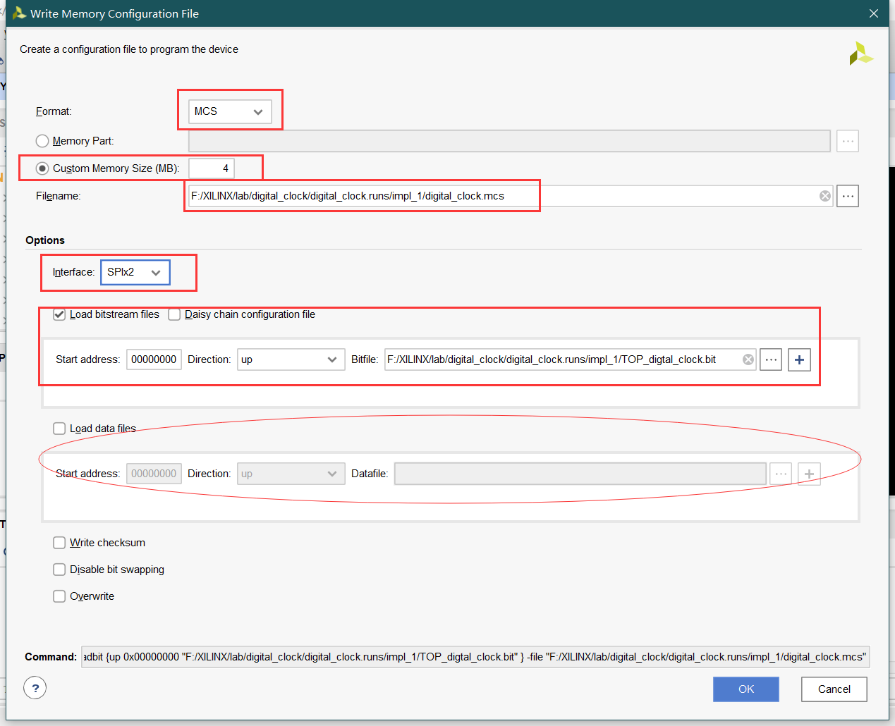 If an error occurs, change the Interface to the value required for the error
Then Add Configuration Memory Device. Three methods:
Method 1.

Method 2.

Method 3.

Next, the following interface appears, select the flash chip.

Select n25q64-3.3v-spi-xi_if an error occurs X2_ X4
Finally, after selecting the chip, the following interface will appear, that is, loading Flash, curing program.
See the following links for the whole project:
Please look forward to ~