1, Experimental principle
1.1 stm32f103c8t6 introduction
STM32F103C8T6 is a 32-bit microcontroller based on Cortex-M3 core launched by St. the hardware is packaged with LQFP48 and belongs to STM32 series of microcontrollers of ST company.
1.2 stm32f103c8t6 lighting principle of running water lamp
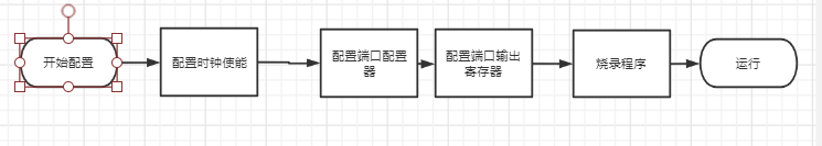
Registers can store data and instructions, and can also perform some specific functions. There are many registers in the stm32 board. If you want to operate the water lamp, you need to operate the corresponding pins. If you want to operate the pins, you need to configure the clock enable, port configuration (high or low) register and port output register of the corresponding pins, That's the next step
1. Because the pins to be operated by the water flow lamp are on the GPIO port, they belong to the AHB bus according to the system structure diagram, so the reset and time control of the ports to be used are controlled by RCC.
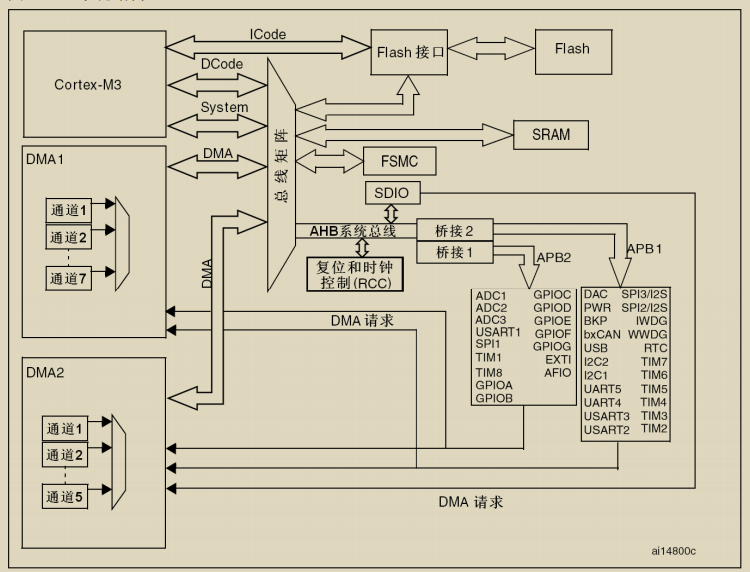
2. Looking at the register group start address table, you can see the address range of RCC, and you can see that the registers to be controlled are all in APB2.
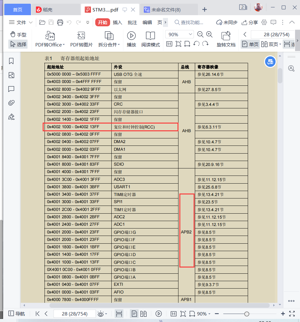
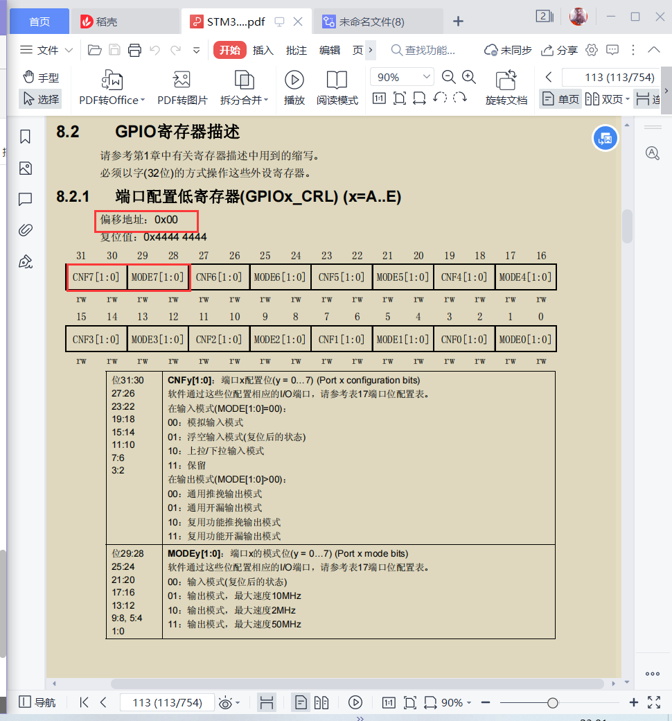
3. Skip to the peripheral clock enable register. The offset is 0x18. In the previous table, you can see that the starting address is 0x4002 1000 and the offset is 0x18, so the address of the register is 0x4002 1018
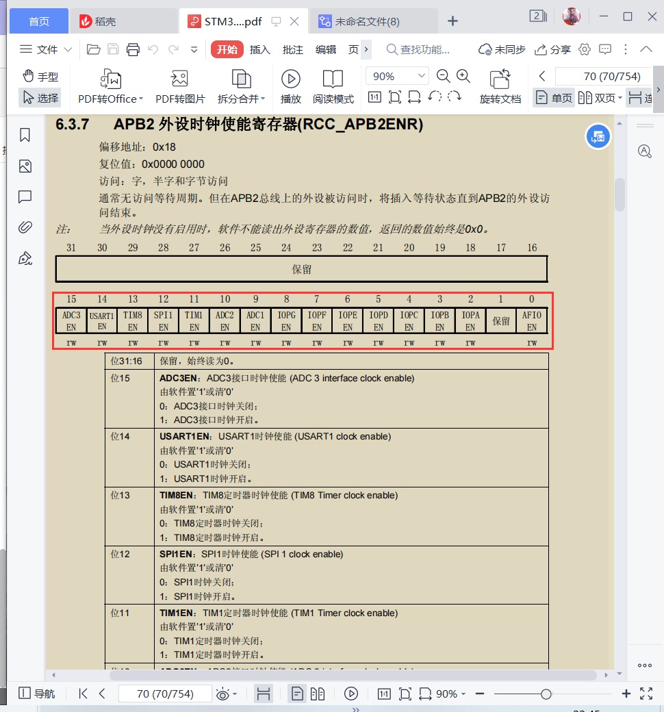
4. Circle processing in the figure is the meaning of each bit in the register. For example, when the third bit, that is, 2, is 1, the clock of GPIOA is turned on. At this time, we can express it in code, taking PA7 pin as an example
#define RCC_AP2ENR	*((unsigned volatile int*)0x40021018) #Clock enable register
RCC_AP2ENR|=1<<2;			//Enable APB2-GPIOA peripheral clock
5. The next step is to configure the port configuration register, which is more critical. It can be found that the clock enable register above is for an area and cannot determine the pin, but this register determines the pin. There are two port configuration registers, namely, the port configuration low register (CRL) and the port configuration high register (CRH), One port is configured every four bits. For example, 11 01 is to select the on function, 01 is to select the mode and determine the maximum speed, but there is one difference. The offset address of the low register is 0x00 and the offset address of the high register is 0x04
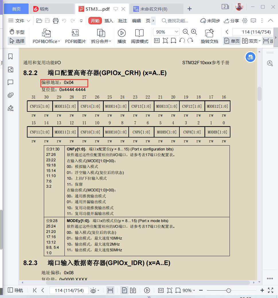
6. Take PA7 as an example, the corresponding port configurator is GPIOA_ The CRL address is the base address + upper offset of GPIOA, which is 0x40010800. This port needs to be turned on, so to make the corresponding bit the corresponding value, I'm 0x20000000 here. Set the push-pull output and the maximum speed to 2Mhz. The following is the corresponding code
#define GPIOA_CRL    *((unsigned volatile int*)0x40010800)
GPIOA_CRL=0x20000000;        //PA7 push pull output, 2Mhz
7. Next, configure the port output register (ORD). You can see that the offset is 0xc, so the address of the register is equal to the base address of the port plus the offset. The output voltage can be controlled by assigning a value in the corresponding bit. 0 is the low voltage and 1 is the high voltage. Take pa7 pin as an example. If you want to output a high voltage, you need to assign 1 in the eighth bit.
The code is as follows. There is bit operation. If you are not familiar with it, please refer to it yourself:
#define	GPIOA_ORD	*((unsigned volatile int*)0x4001080C)
GPIOA_ORD|=1<<7;			//Set the initial light to on
8. Here you can control the led on or off. To realize the running water lamp, you only need to increase the number of lamps and add some delay.
2, Programming implementation
1. First create a project: led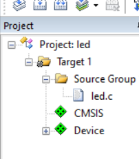
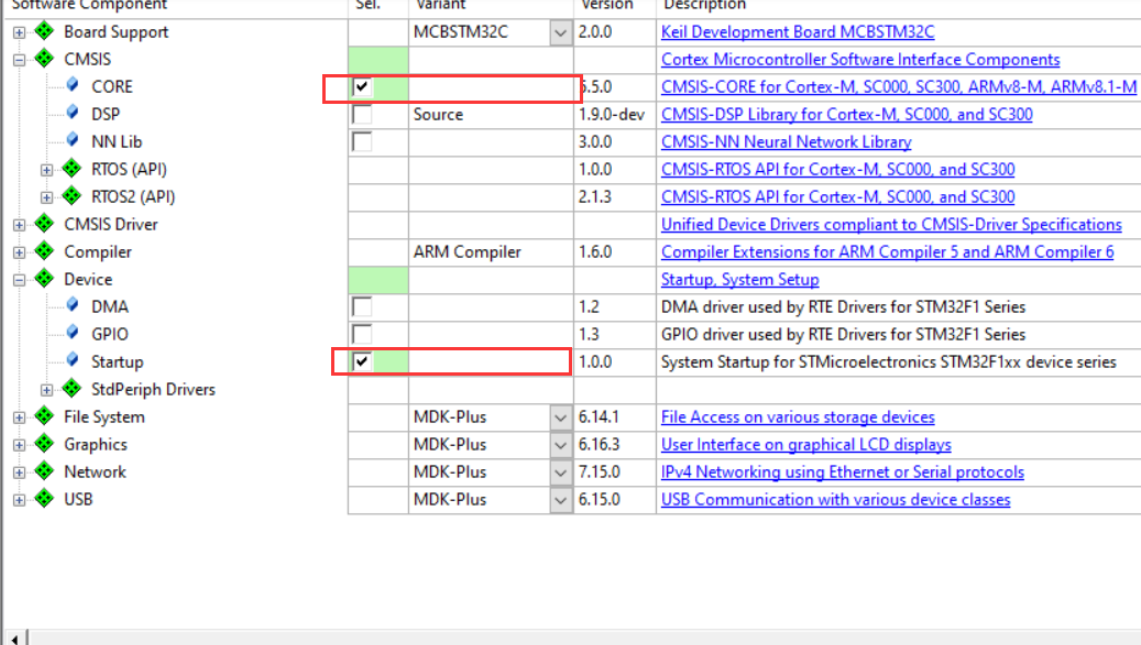
Check the configuration environment
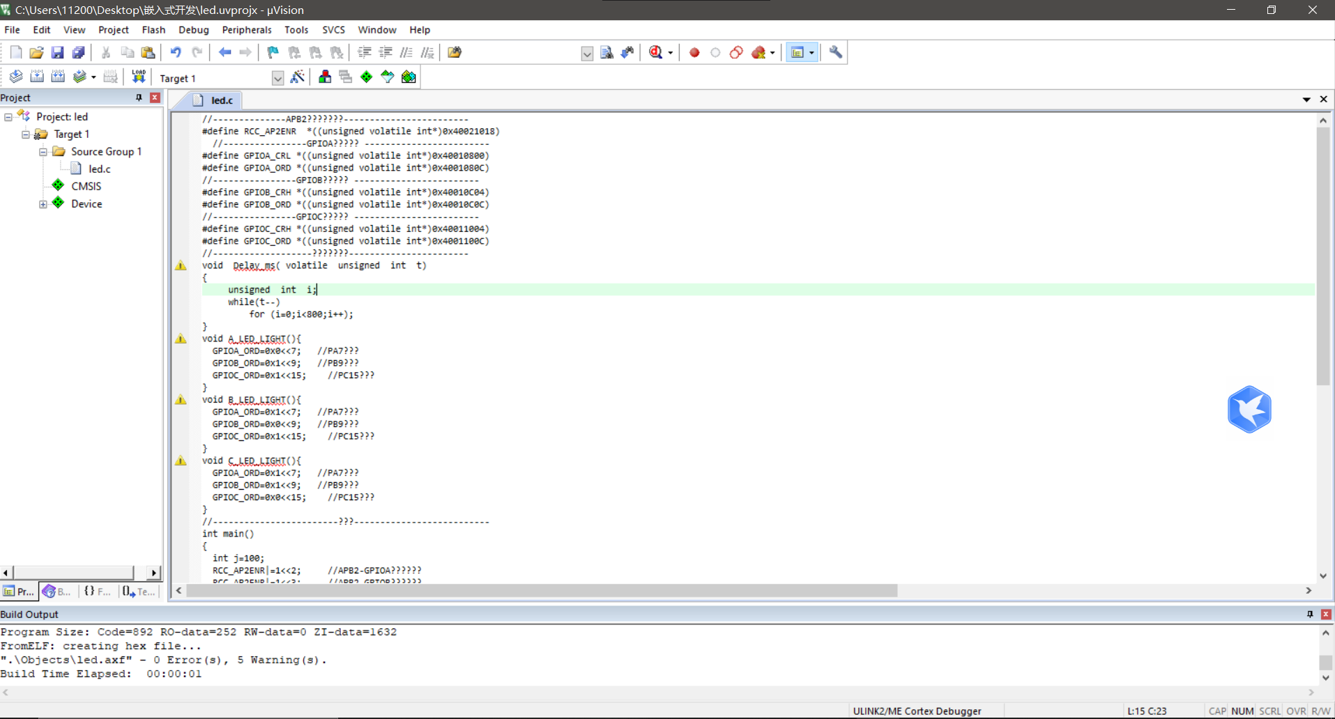
2. Then create a. c file: led.c
Enter code:
//--------------APB2 enable clock register------------------------
#define RCC_AP2ENR	*((unsigned volatile int*)0x40021018)
	//----------------GPIOA configuration register------------------------
#define GPIOA_CRL	*((unsigned volatile int*)0x40010800)
#define	GPIOA_ORD	*((unsigned volatile int*)0x4001080C)
//----------------GPIOB configuration register------------------------
#define GPIOB_CRH	*((unsigned volatile int*)0x40010C04)
#define	GPIOB_ORD	*((unsigned volatile int*)0x40010C0C)
//----------------GPIOC configuration register------------------------
#define GPIOC_CRH	*((unsigned volatile int*)0x40011004)
#define	GPIOC_ORD	*((unsigned volatile int*)0x4001100C)
//-------------------Simple delay function-----------------------
void  Delay_ms( volatile  unsigned  int  t)
{
     unsigned  int  i;
     while(t--)
         for (i=0;i<800;i++);
}
void A_LED_LIGHT(){
	GPIOA_ORD=0x0<<7;		//PA7 low level
	GPIOB_ORD=0x1<<9;		//PB9 high level
	GPIOC_ORD=0x1<<15;		//PC15 high level
}
void B_LED_LIGHT(){
	GPIOA_ORD=0x1<<7;		//PA7 high level
	GPIOB_ORD=0x0<<9;		//PB9 low level
	GPIOC_ORD=0x1<<15;		//PC15 high level
}
void C_LED_LIGHT(){
	GPIOA_ORD=0x1<<7;		//PA7 high level
	GPIOB_ORD=0x1<<9;		//PB9 high level
	GPIOC_ORD=0x0<<15;		//PC15 low level
}
//------------------------Main function--------------------------
int main()
{
	int j=100;
	RCC_AP2ENR|=1<<2;			//APB2-GPIOA peripheral clock enable
	RCC_AP2ENR|=1<<3;			//APB2-GPIOB peripheral clock enable
	RCC_AP2ENR|=1<<4;			//APB2-GPIOC peripheral clock enable
	//These two lines of code can be combined into RCC_ APB2ENR|=1<<3|1<<4;
	GPIOA_CRL&=0x0FFFFFFF;		//Set bit reset
	GPIOA_CRL|=0x20000000;		//PA7 push pull output
	GPIOA_ORD|=1<<7;			//Set PA7 initial light to off

	GPIOB_CRH&=0xFFFFFF0F;		//Set bit reset
	GPIOB_CRH|=0x00000020;		//PB9 push pull output
	GPIOB_ORD|=1<<9;			//Set the initial light to off

	GPIOC_CRH&=0x0FFFFFFF;		//Set bit reset
	GPIOC_CRH|=0x30000000;   	//PC15 push pull output
	GPIOC_ORD|=0x1<<15;			//Set the initial light to off
	while(j)
	{
		A_LED_LIGHT();
		Delay_ms(10000000);
		B_LED_LIGHT();
		Delay_ms(10000000);
		C_LED_LIGHT();
		Delay_ms(10000000);
	}
}
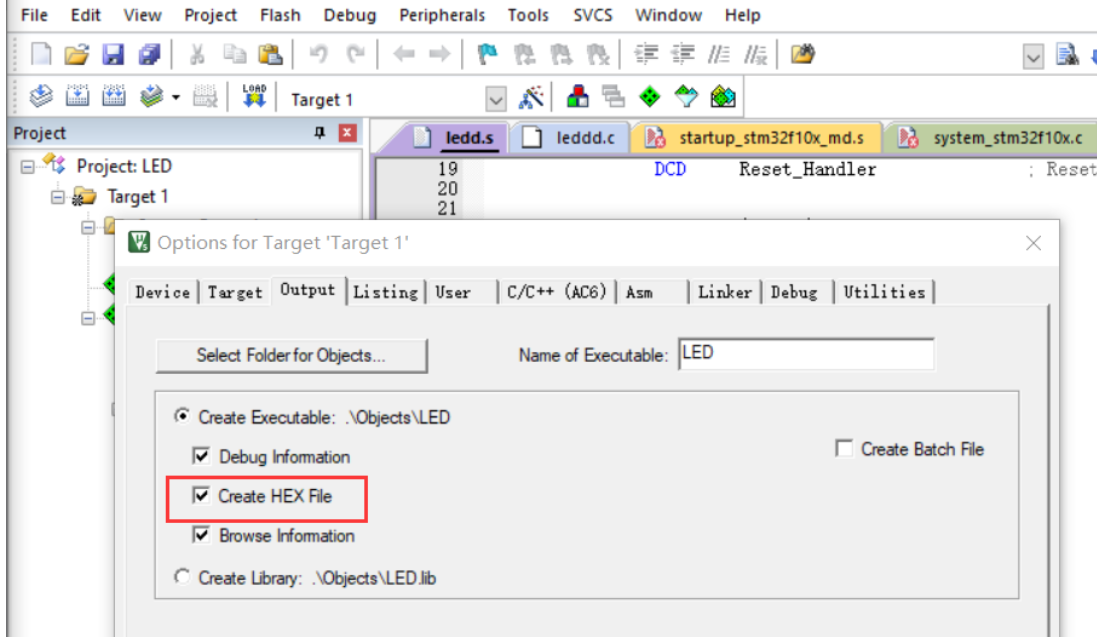
3. After compiling, click the magic wand, and then generate the hex file
4. Download and install the simulation software flymcu according to the online tutorial
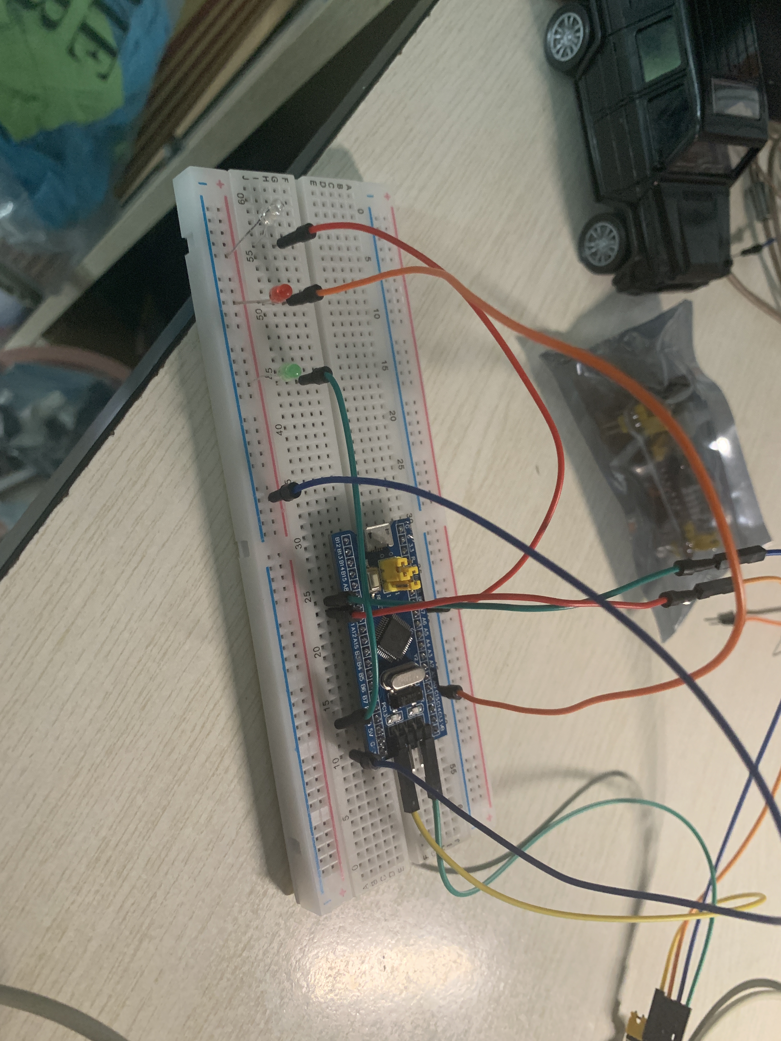
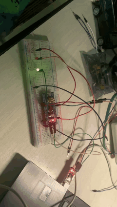
5. Assemble the circuit according to this drawing
6. Check the check and execute after programming, and click start programming (at the same time, check the write option byte when programming to FLASH)
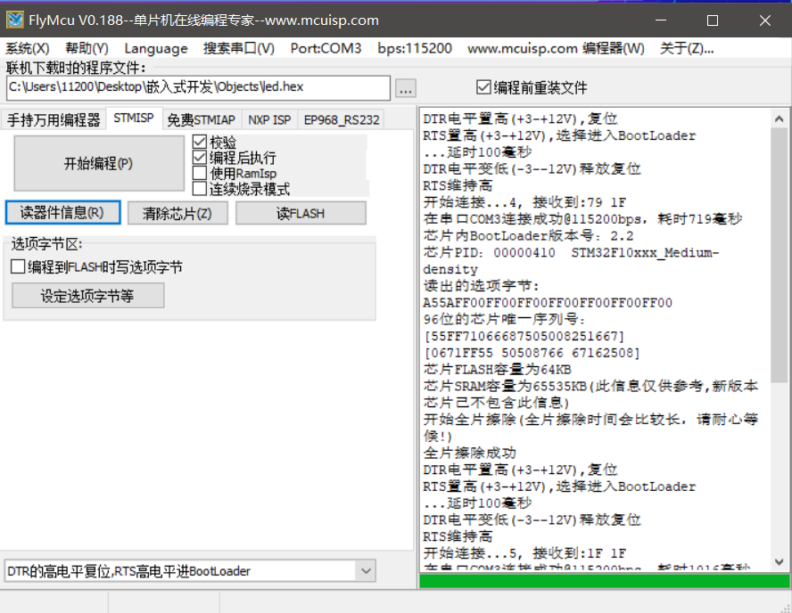
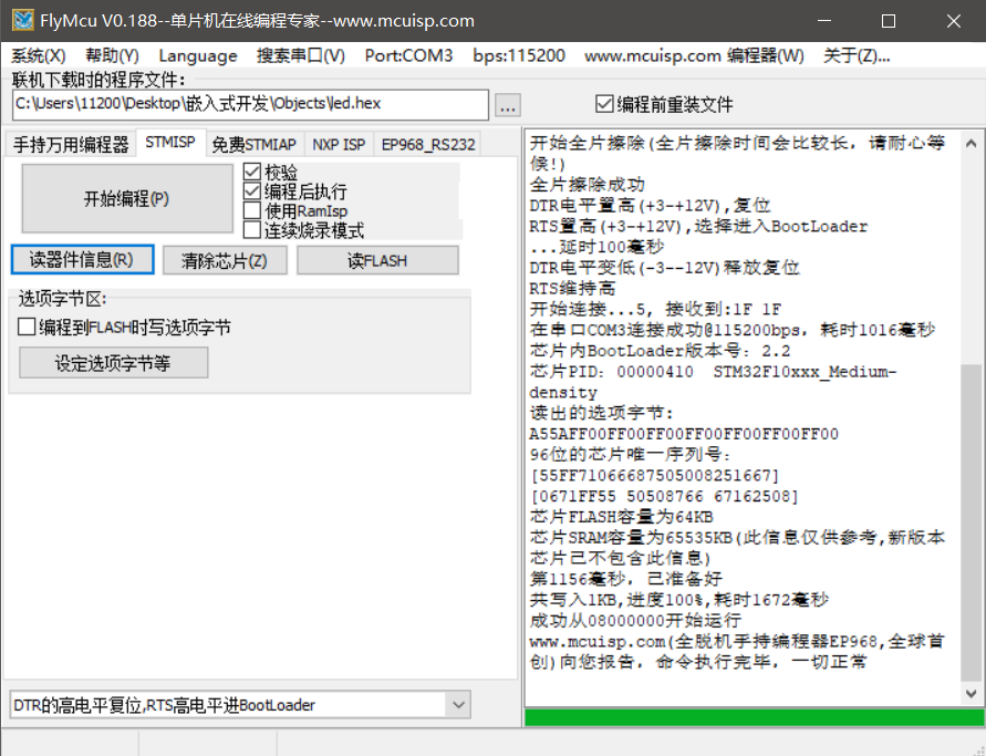
7. Operation
3, Summary
Through the study of this experiment, I have a deeper understanding of the transfer mode of C language call function parameters and the use method of ARM register. In fact, assembly language and C language have a lot in common. We can better understand and master the relevant knowledge of assembly language while learning C language.