catalogue
1, STM32 register rules and IO port introduction
3.3 burning: connection between STM32 and PC
4, Assembly language implementation
1, STM32 register rules and IO port introduction
What this blog will achieve is to control the three IO ports on the STM32 development board to achieve an effect similar to water lamp. The key of this experiment is how to control the IO port output of STM32. After understanding how the IO port of STM32 outputs, you can realize the water lamp. Through this study, you will initially master the use of STM32 basic IO port, which is the first step towards STM32.
The IO port of STM32 can be configured into the following 8 modes by software:
1. Input float
2. Input pull-up
3. Input drop-down
4. Analog input
5. Open drain output
6. Push pull output
7. Push pull multiplexing function
8. Open drain multiplexing function
Each IO port can be programmed freely, but the IO port register must be accessed as a 32-bit word. Each IO port of STM32 has 7 registers to control. They are: two 32-bit port configuration registers CRL and CRH in configuration mode; Two 32-bit data registers IDR and ODR; 1 32-bit set / reset register BSRR; A 16 bit reset register BRR; 1 32-bit latch register LCKR; Here we only introduce a few commonly used registers. There are only four commonly used IO port registers: CRL, CRH, IDR and ODR.
CRL and CRH control the mode and output rate of each IO port. The IO port configuration table of STM32 is shown in the table below:
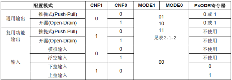
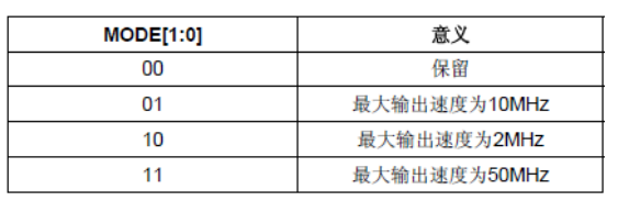
STM32 output mode configuration is shown in the table:
Next, let's look at the description of the port low configuration register CRL, as shown in the figure:
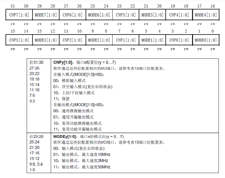 The reset value of this register is 0X4444 4444. As can be seen from figure 6.1.1, the reset value actually configures the port to float input MODE. It can also be seen from the above figure that the CRL of STM32 controls the low 8-bit MODE of each group of IO ports (A~G). The bits of each IO port occupy 4 bits of the CRL. The high two bits are CNF and the low two bits are MODE. Here we can remember several common configurations, such as 0X0 for analog input MODE (for ADC), 0X3 for push-pull output MODE (for output port, 50M rate), 0X8 for up / down input MODE (for input port), and 0XB for multiplexing output (using the second function of IO port, 50M rate).
The function of CRH is exactly the same as that of CRL, except that CRL controls the low 8-bit output port, while CRH controls the high 8-bit output port. We will not introduce CRH in detail here. For example, we need to set 11 bits of PORTC as pull-up input and 12 bits as push-pull output. The code is as follows:
GPIOC->CRH&=0XFFF00FFF;//Clear the original settings of these two bits without affecting the settings of other bits

GPIOC->CRH|=0X00038000; //PC11 input, PC12 output

GPIOC->ODR=1<<11; //PC11 pull up
Through the configuration of these three sentences, we set PC11 as pull-up input and PC12 as push-pull output.
IDR is a port input data register that uses only the low 16 bits. This register is read-only and can only be read out in the form of 16 bits. The description of each bit of the register is shown in the figure:
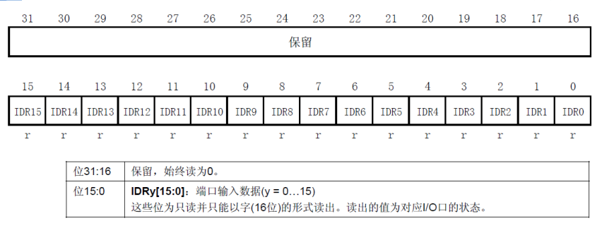
To know the status of an IO port, you just need to read this register and look at the status of a bit. It is relatively simple to use.
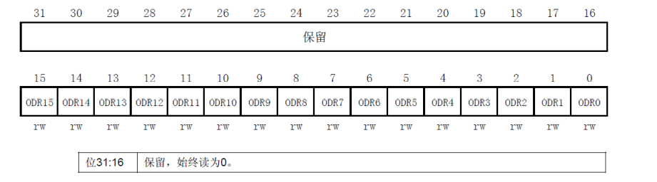
ODR is a port output data register, which only uses the low 16 bits. The register is read-write, and the data read from the register can be used to judge the output state of the Current IO port. Writing data to the register can control the output level of an IO port. The description of each bit of the register is shown in the figure:
Knowing these registers, we can start the real design of the water lamp experiment.
2, Hardware connection design
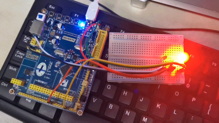
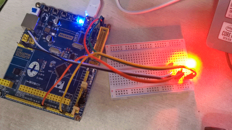
According to the requirements of the topic, I use gpiob, gpioc and gpiod ports to control the LED lights. After querying the STM32 data manual, I select PB6, PC6 and PD2 pins to connect the red, green and blue lights respectively (because I only have three small lights of red, green and yellow, in the actual hardware, I will use the yellow light instead of the blue light)
3, Software design
3.1 configure IO port
We first need to configure the IO port. The configuration method we use here is to use registers. Change the value of the IO port by configuring the value of the register.
led.h
#ifndef __LED_H
#define __LED_H
#include "sys.h"

//LED port definition
#define LED0 BIT_ Addr (gpiob_odr_addr, 6) / / pb6 output
#define LED1 BIT_ADDR(GPIOC_ODR_Addr,6) 	  //  PC6 output
#define LED2 BIT_ADDR(GPIOD_ODR_Addr,2) 	  //  PD2 output

void LED_Init(void);	//initialization
#endif
led.c
#include "sys.h"
#include "led.h"

//Initialize PB6, PC6 and PD2 as output ports and enable the clocks of these three ports
//LEDIO initialization
void LED_Init(void)
{
	RCC->APB2ENR|=1<<3;    //Enable PORTB clock
	RCC->APB2ENR|=1<<4;    //Enable PORTC clock
	RCC->APB2ENR|=1<<5;    //Enable PORTD clock

	GPIOB->CRL&=0XF0FFFFFF; //PB6 reset
	GPIOB->CRL|=0X03000000; //PB6 push pull output
    GPIOB->ODR|=1<<6;       //PB6 output high

	GPIOC->CRL&=0XF0FFFFFF; //PC6 reset
	GPIOC->CRL|=0X03000000; //PC6 push pull output
	GPIOC->ODR|=1<<6;      //PC6 output high

	GPIOD->CRL&=0XFFFFF0FF; //PD2 reset
	GPIOD->CRL|=0X00000300;//PD2 push pull output
    GPIOD->ODR|=1<<2;      //PD2 output high

}
3.2 writing main functions
test.c
#include "sys.h"
#include "led.h"

void delay(unsigned int i)   //Simple delay function
{
	unsigned char j;
	unsigned char k;
	for(;i>0;i--)
		for(j=500; j>0; j--)
	       for(k =200; k>0; k--);
}

int main(void)
{

	LED_Init();		  	 	//Initialize the hardware interface to the LED
	while(1)
	{

		LED0=0;  //Light on
		LED1=1;  //Lights out
		LED2=1;
		delay(20);  //delayed
		LED0=1;
		LED1=0;
		LED2=1;
		delay(20);
	    LED0=1;
		LED1=1;
		LED2=0;
		delay(20);

	}
}
3.3 burning: connection between STM32 and PC
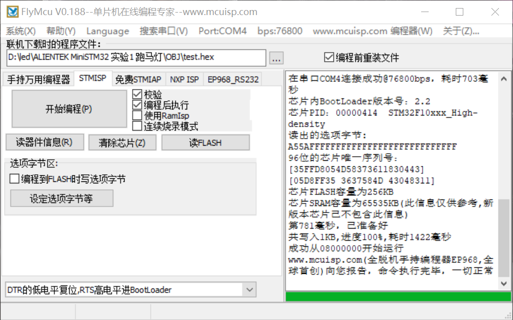
With the help of flymcu download software, test.hex can be loaded, and the software data can also be downloaded on the network disk. Here I use flymcu.
3.4 effect demonstration
4, Assembly language implementation
code:
RCC_APB2ENR EQU 0x40021018

GPIOA_CRH EQU   0x40010804
GPIOA_ODR EQU   0x4001080C

GPIOB_CRL EQU   0x40010C00    ;Register mapping
GPIOB_ODR EQU   0x40010C0C

GPIOC_CRH EQU   0x40011004
GPIOC_ODR EQU   0x4001100C


Stack_Size      EQU     0x00000400

                AREA    STACK, NOINIT, READWRITE, ALIGN=3
					;NOINIT:  = NO Init,Not initialized. READWRITE : Readable and writable. ALIGN =3 : 2^3 Alignment, i.e. 8-byte alignment.
Stack_Mem       SPACE   Stack_Size
__initial_sp

                AREA    RESET, DATA, READONLY

__Vectors       DCD     __initial_sp
                DCD     Reset_Handler


                AREA    |.text|, CODE, READONLY

                THUMB
                REQUIRE8
                PRESERVE8

                ENTRY
Reset_Handler


MainLoop		BL LED2_Init
                BL LED2_ON
                BL Delay             ;LED2 The lamp flashes
                BL LED2_OFF
                BL Delay

				BL LED1_Init
				BL LED1_ON
                BL Delay             ;LED1 The lamp flashes
                BL LED1_OFF
                BL Delay

                BL LED3_Init
				BL LED3_ON
                BL Delay            ;LED3 The lamp flashes
                BL LED3_OFF
                BL Delay

                B MainLoop


LED1_Init
                PUSH {R0,R1, LR}        ;R0,R1,LR Put the values in the stack

                LDR R0,=RCC_APB2ENR      ;LDR Is to load the address into the register(such as R0).
                ORR R0,R0,#0x08         ; Turn on the clock of port GPIOB, ORR operates by bit or, 01000 will set the second position of R0 to 1, and other bits remain unchanged
                LDR R1,=RCC_APB2ENR
                STR R0,[R1]             ;STR Is to store the value in the address indicated by the register r0 The value stored in rcc register
				;The above part of the assembly code controls the clock


                LDR R0,=GPIOB_CRL
                ORR R0,R0,#0X00000020   ;GPIOB_Pin_1 is configured as universal push-pull output; pb1 is turned on, so it is 2, 0010. It is a push-pull output mode, and the maximum speed is 2mhz
                LDR R1,=GPIOB_CRL
                STR R0,[R1]

                LDR R0,=GPIOB_ODR
                BIC R0,R0,#0X00000002      ;BIC reverses the immediate data first, and then compares it by bit
                LDR R1,=GPIOB_ODR          ;GPIOB_Pin_1 The output is 0;from r1 control ord register
                STR R0,[R1]                 ;take ord The value of the register becomes r0 Value of

                POP {R0,R1,PC}             ;Store the previously stored in the stack R0,R1,LR Value returned to R0,R1,PC


LED1_OFF
                PUSH {R0,R1, LR}

                LDR R0,=GPIOB_ODR
                BIC R0,R0,#0X00000002    ; Because it is PB1, it corresponds to binary 0010;GPIOB_Pin_1 output is 0, LED1 is off
			    LDR R1,=GPIOB_ODR
                STR R0,[R1]

                POP {R0,R1,PC}

LED1_ON
                PUSH {R0,R1, LR}

                 LDR R0,=GPIOB_ODR
                ORR R0,R0,#0X00000002    ;GPIOB_Pin_1 output is 1, LED1 is on
                 LDR R1,=GPIOB_ODR
                STR R0,[R1]
                POP {R0,R1,PC}


LED2_Init
                PUSH {R0,R1, LR};R0,R1,LR Put the values in the stack

                LDR R0,=RCC_APB2ENR
                ORR R0,R0,#0x04 		   ; Turn on the clock of GPIOA
                LDR R1,=RCC_APB2ENR
                STR R0,[R1]

                LDR R0,=GPIOA_CRH
                ORR R0,R0,#0X00020000   ;GPIOA_Pin_12 is configured as a universal push-pull output
                LDR R1,=GPIOA_CRH
                STR R0,[R1]

                LDR R0,=GPIOA_ODR
                BIC R0,R0,#0X00001000
                LDR R1,=GPIOA_ODR            ;GPIOA_Pin_12 The output is 0
                STR R0,[R1]

                POP {R0,R1,PC}

LED2_OFF
                PUSH {R0,R1, LR}

               LDR R0,=GPIOA_ODR
               BIC R0,R0,#0X00001000        ;GPIOA_Pin_12 output is 0, LED2 is off
			    LDR R1,=GPIOA_ODR
                STR R0,[R1]

                POP {R0,R1,PC}

LED2_ON
                PUSH {R0,R1, LR}

                LDR R0,=GPIOA_ODR
                ORR R0,R0,#0X00001000     ;GPIOA_Pin_12 output is 1, LED2 is on
				 LDR R1,=GPIOA_ODR
                STR R0,[R1]

				 POP {R0,R1,PC}


LED3_Init
                PUSH {R0,R1, LR}

                LDR R0,=RCC_APB2ENR
                ORR R0,R0,#0x10 		    ; Turn on the clock of GPIOC
                LDR R1,=RCC_APB2ENR
                STR R0,[R1]

                LDR R0,=GPIOC_CRH
                ORR R0,R0,#0X02000000   ;GPIOC_Pin_14 is configured as a universal push-pull output
                LDR R1,=GPIOC_CRH
                STR R0,[R1]

                LDR R0,=GPIOC_ODR
                BIC R0,R0,#0X00004000   ;GPIOC_Pin_14 output is 0
                LDR R1,=GPIOC_ODR
                STR R0,[R1]

                POP {R0,R1,PC}

LED3_OFF
                PUSH {R0,R1, LR}

                LDR R0,=GPIOC_ODR
                BIC R0,R0,#0X00004000  ;GPIOC_Pin_14 output is 0, LED3 goes out
			    LDR R1,=GPIOC_ODR
                STR R0,[R1]

                POP {R0,R1,PC}

LED3_ON
                PUSH {R0,R1, LR}

                 LDR R0,=GPIOC_ODR
                ORR R0,R0,#0X00004000   ;GPIOC_Pin_14 output is 1, LED3 is on
                 LDR R1,=GPIOC_ODR
                STR R0,[R1]

                POP {R0,R1,PC}

Delay
                PUSH {R0,R1, LR}

                MOVS R0,#0
                MOVS R1,#0
                MOVS R2,#0

DelayLoop0
                ADDS R0,R0,#1

                CMP R0,#300
                BCC DelayLoop0

                MOVS R0,#0
                ADDS R1,R1,#1
                CMP R1,#300
                BCC DelayLoop0

                MOVS R0,#0
                MOVS R1,#0
                ADDS R2,R2,#1
                CMP R2,#15
                BCC DelayLoop0

                POP {R0,R1,PC}

                END
The compilation and burning method is the same as above, and the effect is displayed
5, References
[embedded 08] detailed explanation of STM32F103C8T6 register mode lighting LED water lamp with the help of bread board_ Poof poof jar blog - CSDN blog https://blog.csdn.net/qq_46467126/article/details/120791793stm32 register introduction, address search, and direct operation register_ Geekyatao CSDN blog_ stm32 registerhttps://blog.csdn.net/geek_monkey/article/details/86291377Learn STM32 from zero (I) -- register operation GPIO_ Linax's blog - CSDN blog register operation GPIO port 1.ARM introduction 2. Introduction to development board 2.1 software installation 2.2 project establishment bus architecture and clock tree GPIO port operation using register: Lighting LED lamp 1. Introduction to ARM 1. Today we learn the book STM32 microcontroller based on ARM cortex-m3; First of all, we should understand the meaning of these terms: ARM: is the name of a company - designing chip kernel architecture - designing CPU cortex -
 https://blog.csdn.net/qq_38639426/article/details/88625547