catalogue
1, Understand serial communication
1. What is serial communication
2. Serial communication protocol
2, STM32 uses the serial port to send "hello windows" to the host computer
1, Understand serial communication
1. What is serial communication
Serial communication refers to a communication mode in which data is transmitted bit by bit between peripherals and computers through data lines, ground wires and control lines. This communication mode uses less data lines, which can save the communication cost in long-distance communication, but its transmission speed is lower than parallel transmission.
2. Serial communication protocol
In computer science, most complex problems can be simplified by layering. For example, the chip is divided into core layer and on-chip peripherals; STM32 standard library is the software layer between register and user code. We also understand the communication protocol in a hierarchical way. The most basic thing is to divide it into physical layer and protocol layer. In short, the physical layer specifies whether we communicate with our mouth or limbs, and the protocol layer specifies whether we communicate in Chinese or English. The physical layer specifies the characteristics of mechanical and electronic functional parts in the communication system to ensure the transmission of original data in physical media, eg: RS232, TTL high and low levels. The protocol layer mainly specifies the communication logic and unifies the data packaging and unpacking standards of both sending and receiving sides. Eg: serial port data packet: start bit, data bit (8bit), check bit and stop bit.
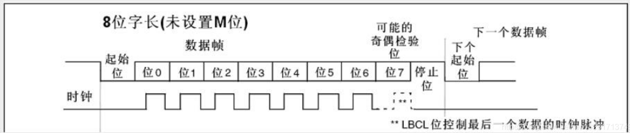
Start bit:
It is in the logic "1" state when there is no data transmission on the communication line. When the transmitting device sends a character data, it first sends a logic "0" signal, and this logic low level is the start bit (falling edge). The start bit is transmitted to the receiving device through the communication line. When the receiving device detects this logic low level, it starts to prepare to receive the data signal. Therefore, the function of the start bit is to indicate the beginning of character transmission.
Data bits:
This is a parameter that measures the actual data bits in communication. When the computer sends a packet, the actual data will not be 8 bits, and the standard values are 5, 7 and 8 bits. How you set it depends on the message you want to send. For example, the standard ascii code is 0 ~ 127 (7 bits). The extended ASCII code is 0 ~ 255 (8 bits). If the data uses simple text (standard ascii code), each packet uses 7 bits of data. Each packet refers to a byte, including start / stop bits, data bits and parity bits. Since the actual data bits depend on the selection of the communication protocol, the term "packet" refers to any communication situation.
Stop bit:
Used to represent the last bit of a single package. Typical values are 1, 1.5 and 2 bits. Because the data is timed on the transmission line and each device has its own clock, there may be a small synchronization between the two devices in the communication. Therefore, the stop bit not only indicates the end of transmission, but also provides an opportunity for the computer to correct clock synchronization. The more bits applicable to stop bits, the greater the tolerance of different clock synchronization, but the slower the data transmission rate.
Parity bit:
A simple error detection method in serial communication. There are four error detection methods: even, odd, high and low. Of course, it is OK to have no check bit. For even and odd parity, the serial port will set the parity bit (one bit after the data bit) and use a value to ensure that the transmitted data has even or odd logical high bits. For example, if the data is 011, for even parity, the parity bit is 0 to ensure that the number of digits with high logic is even. If it is an odd check, the check bit is 1, so there are three logical high bits. The high and low bits do not really check the data. Simply set the logic high or logic low check. In this way, the receiving device can know the state of one bit and have the opportunity to judge whether there is noise interfering with the communication or whether the transmission and reception data are not synchronized.
2, STM32 uses the serial port to send "hello windows" to the host computer
1. Wiring:
GND-G
3V3-3.3
RXD-A10
TXD-A9
TXD: transmit data output pin
RXD: receive data output pin
2. Code
. s file code
;RCC Register address mapping
RCC_BASE EQU 0x40021000
RCC_CR EQU (RCC_BASE + 0x00)
RCC_CFGR EQU (RCC_BASE + 0x04)
RCC_CIR EQU (RCC_BASE + 0x08)
RCC_APB2RSTR EQU (RCC_BASE + 0x0C)
RCC_APB1RSTR EQU (RCC_BASE + 0x10)
RCC_AHBENR EQU (RCC_BASE + 0x14)
RCC_APB2ENR EQU (RCC_BASE + 0x18)
RCC_APB1ENR EQU (RCC_BASE + 0x1C)
RCC_BDCR EQU (RCC_BASE + 0x20)
RCC_CSR EQU (RCC_BASE + 0x24)
;AFIO Register address mapping
AFIO_BASE EQU 0x40010000
AFIO_EVCR EQU (AFIO_BASE + 0x00)
AFIO_MAPR EQU (AFIO_BASE + 0x04)
AFIO_EXTICR1 EQU (AFIO_BASE + 0x08)
AFIO_EXTICR2 EQU (AFIO_BASE + 0x0C)
AFIO_EXTICR3 EQU (AFIO_BASE + 0x10)
AFIO_EXTICR4 EQU (AFIO_BASE + 0x14)
;GPIOA Register address mapping
GPIOA_BASE EQU 0x40010800
GPIOA_CRL EQU (GPIOA_BASE + 0x00)
GPIOA_CRH EQU (GPIOA_BASE + 0x04)
GPIOA_IDR EQU (GPIOA_BASE + 0x08)
GPIOA_ODR EQU (GPIOA_BASE + 0x0C)
GPIOA_BSRR EQU (GPIOA_BASE + 0x10)
GPIOA_BRR EQU (GPIOA_BASE + 0x14)
GPIOA_LCKR EQU (GPIOA_BASE + 0x18)
;GPIO C Mouth control
GPIOC_BASE EQU 0x40011000
GPIOC_CRL EQU (GPIOC_BASE + 0x00)
GPIOC_CRH EQU (GPIOC_BASE + 0x04)
GPIOC_IDR EQU (GPIOC_BASE + 0x08)
GPIOC_ODR EQU (GPIOC_BASE + 0x0C)
GPIOC_BSRR EQU (GPIOC_BASE + 0x10)
GPIOC_BRR EQU (GPIOC_BASE + 0x14)
GPIOC_LCKR EQU (GPIOC_BASE + 0x18)
;Serial port 1 control
USART1_BASE EQU 0x40013800
USART1_SR EQU (USART1_BASE + 0x00)
USART1_DR EQU (USART1_BASE + 0x04)
USART1_BRR EQU (USART1_BASE + 0x08)
USART1_CR1 EQU (USART1_BASE + 0x0c)
USART1_CR2 EQU (USART1_BASE + 0x10)
USART1_CR3 EQU (USART1_BASE + 0x14)
USART1_GTPR EQU (USART1_BASE + 0x18)
;NVIC Register address
NVIC_BASE EQU 0xE000E000
NVIC_SETEN EQU (NVIC_BASE + 0x0010)
;SETENA Starting address of register array
NVIC_IRQPRI EQU (NVIC_BASE + 0x0400)
;Start address of interrupt priority register array
NVIC_VECTTBL EQU (NVIC_BASE + 0x0D08)
;Address of vector table offset register
NVIC_AIRCR EQU (NVIC_BASE + 0x0D0C)
;Address of application interrupt and reset control register
SETENA0 EQU 0xE000E100
SETENA1 EQU 0xE000E104
;SysTick Register address
SysTick_BASE EQU 0xE000E010
SYSTICKCSR EQU (SysTick_BASE + 0x00)
SYSTICKRVR EQU (SysTick_BASE + 0x04)
;FLASH Buffer register address image
FLASH_ACR EQU 0x40022000
;SCB_BASE EQU (SCS_BASE + 0x0D00)
MSP_TOP EQU 0x20005000
;Starting value of main stack
PSP_TOP EQU 0x20004E00
;Process stack start value
BitAlias_BASE EQU 0x22000000
;Bit alias area start address
Flag1 EQU 0x20000200
b_flas EQU (BitAlias_BASE + (0x200*32) + (0*4))
;Bit address
b_05s EQU (BitAlias_BASE + (0x200*32) + (1*4))
;Bit address
DlyI EQU 0x20000204
DlyJ EQU 0x20000208
DlyK EQU 0x2000020C
SysTim EQU 0x20000210
;Constant definition
Bit0 EQU 0x00000001
Bit1 EQU 0x00000002
Bit2 EQU 0x00000004
Bit3 EQU 0x00000008
Bit4 EQU 0x00000010
Bit5 EQU 0x00000020
Bit6 EQU 0x00000040
Bit7 EQU 0x00000080
Bit8 EQU 0x00000100
Bit9 EQU 0x00000200
Bit10 EQU 0x00000400
Bit11 EQU 0x00000800
Bit12 EQU 0x00001000
Bit13 EQU 0x00002000
Bit14 EQU 0x00004000
Bit15 EQU 0x00008000
Bit16 EQU 0x00010000
Bit17 EQU 0x00020000
Bit18 EQU 0x00040000
Bit19 EQU 0x00080000
Bit20 EQU 0x00100000
Bit21 EQU 0x00200000
Bit22 EQU 0x00400000
Bit23 EQU 0x00800000
Bit24 EQU 0x01000000
Bit25 EQU 0x02000000
Bit26 EQU 0x04000000
Bit27 EQU 0x08000000
Bit28 EQU 0x10000000
Bit29 EQU 0x20000000
Bit30 EQU 0x40000000
Bit31 EQU 0x80000000
;Vector table
AREA RESET, DATA, READONLY
DCD MSP_TOP ;Initialize main stack
DCD Start ;Reset vector
DCD NMI_Handler ;NMI Handler
DCD HardFault_Handler ;Hard Fault Handler
DCD 0
DCD 0
DCD 0
DCD 0
DCD 0
DCD 0
DCD 0
DCD 0
DCD 0
DCD 0
DCD 0
DCD SysTick_Handler ;SysTick Handler
SPACE 20 ;Reserved space 20 bytes
;Code snippet
AREA |.text|, CODE, READONLY
;Main program start
ENTRY
;Instructs the program to execute from here
Start
;Clock system settings
ldr r0, =RCC_CR
ldr r1, [r0]
orr r1, #Bit16
str r1, [r0]
;Enable external crystal oscillator
;Start external 8 M Crystal oscillator
ClkOk
ldr r1, [r0]
ands r1, #Bit17
beq ClkOk
;Wait for the external crystal oscillator to be ready
ldr r1,[r0]
orr r1,#Bit17
str r1,[r0]
;FLASH Buffer
ldr r0, =FLASH_ACR
mov r1, #0x00000032
str r1, [r0]
;set up PLL The PLL magnification is 7,HSE Input no frequency division
ldr r0, =RCC_CFGR
ldr r1, [r0]
orr r1, #(Bit18 :OR: Bit19 :OR: Bit20 :OR: Bit16 :OR: Bit14)
orr r1, #Bit10
str r1, [r0]
;start-up PLL Phase locked loop
ldr r0, =RCC_CR
ldr r1, [r0]
orr r1, #Bit24
str r1, [r0]
PllOk
ldr r1, [r0]
ands r1, #Bit25
beq PllOk
;choice PLL Clock as system clock
ldr r0, =RCC_CFGR
ldr r1, [r0]
orr r1, #(Bit18 :OR: Bit19 :OR: Bit20 :OR: Bit16 :OR: Bit14)
orr r1, #Bit10
orr r1, #Bit1
str r1, [r0]
;other RCC Related settings
ldr r0, =RCC_APB2ENR
mov r1, #(Bit14 :OR: Bit4 :OR: Bit2)
str r1, [r0]
;IO port settings
ldr r0, =GPIOC_CRL
ldr r1, [r0]
orr r1, #(Bit28 :OR: Bit29)
;PC.7 Output mode,Maximum speed 50 MHz
and r1, #(~Bit30 & ~Bit31)
;PC.7 Universal push-pull output mode
str r1, [r0]
;PA9 Serial port 0 transmitting pin
ldr r0, =GPIOA_CRH
ldr r1, [r0]
orr r1, #(Bit4 :OR: Bit5)
;PA.9 Output mode,Maximum speed 50 MHz
orr r1, #Bit7
and r1, #~Bit6
;10: Multiplexing function push-pull output mode
str r1, [r0]
ldr r0, =USART1_BRR
mov r1, #0x271
str r1, [r0]
;Configure baud rate-> 115200
ldr r0, =USART1_CR1
mov r1, #0x200c
str r1, [r0]
;USART Module total enable send and receive enable
;71 02 00 00 2c 20 00 00
;AFIO Parameter setting
;Systick Parameter setting
ldr r0, =SYSTICKRVR
;Systick Initial installation value
mov r1, #9000
str r1, [r0]
ldr r0, =SYSTICKCSR
;set up,start-up Systick
mov r1, #0x03
str r1, [r0]
;NVIC
;ldr r0, =SETENA0
;mov r1, 0x00800000
;str r1, [r0]
;ldr r0, =SETENA1
;mov r1, #0x00000100
;str r1, [r0]
;Switch to user level line program mode
ldr r0, =PSP_TOP
;Initialize thread stack
msr psp, r0
mov r0, #3
msr control, r0
;initialization SRAM register
mov r1, #0
ldr r0, =Flag1
str r1, [r0]
ldr r0, =DlyI
str r1, [r0]
ldr r0, =DlyJ
str r1, [r0]
ldr r0, =DlyK
str r1, [r0]
ldr r0, =SysTim
str r1, [r0]
;Main cycle
main
ldr r0, =Flag1
ldr r1, [r0]
tst r1, #Bit1
;SysTick Generate 0.5s,Set bit 1
beq main ;0.5s The flag is not set yet
;0.5s The flag has been set
ldr r0, =b_05s
;Bit band operation reset 0.5s sign
mov r1, #0
str r1, [r0]
bl LedFlas
mov r0, #'H'
bl send_a_char
mov r0, #'e'
bl send_a_char
mov r0, #'l'
bl send_a_char
mov r0, #'l'
bl send_a_char
mov r0, #'o'
bl send_a_char
mov r0, #' '
bl send_a_char
mov r0, #'w'
bl send_a_char
mov r0, #'o'
bl send_a_char
mov r0, #'r'
bl send_a_char
mov r0, #'l'
bl send_a_char
mov r0, #'d'
bl send_a_char
mov r0, #'\n'
bl send_a_char
b main
;Subroutine serial port 1 sends a character
send_a_char
push {r0 - r3}
ldr r2, =USART1_DR
str r0, [r2]
b1
ldr r2, =USART1_SR
ldr r2, [r2]
tst r2, #0x40
beq b1
;Send complete(Transmission complete)wait for
pop {r0 - r3}
bx lr
;subroutine led twinkle
LedFlas
push {r0 - r3}
ldr r0, =Flag1
ldr r1, [r0]
tst r1, #Bit0
;bit0 Flashing flag bit
beq ONLED ;Open for 0 led lamp
;Off for 1 led lamp
ldr r0, =b_flas
mov r1, #0
str r1, [r0]
;The flashing flag position is 0,The next status is on
;PC.7 Output 0
ldr r0, =GPIOC_BRR
ldr r1, [r0]
orr r1, #Bit7
str r1, [r0]
b LedEx
ONLED
;Open for 0 led lamp
ldr r0, =b_flas
mov r1, #1
str r1, [r0]
;The flashing flag position is 1,The next status is off
;PC.7 Output 1
ldr r0, =GPIOC_BSRR
ldr r1, [r0]
orr r1, #Bit7
str r1, [r0]
LedEx
pop {r0 - r3}
bx lr
;Abnormal program
NMI_Handler
bx lr
HardFault_Handler
bx lr
SysTick_Handler
ldr r0, =SysTim
ldr r1, [r0]
add r1, #1
str r1, [r0]
cmp r1, #500
bcc TickExit
mov r1, #0
str r1, [r0]
ldr r0, =b_05s
;The clock tick counter is set to 0 when it is greater than or equal to 500 times of clearing.5s Flag bit
;Bit band operation set 1
mov r1, #1
str r1, [r0]
TickExit
bx lr
ALIGN
;By using zero or null instructions NOP fill,Aligns the current position with a specified boundary
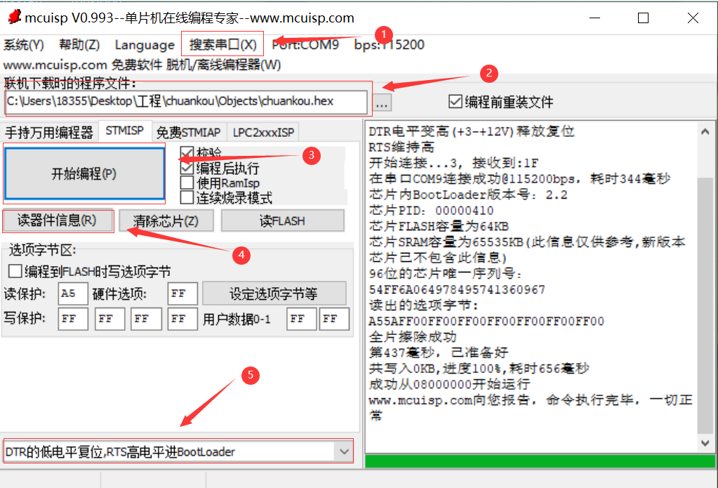
END3. Burn in board
Click and observe according to the following sequence number to burn the program into the board:
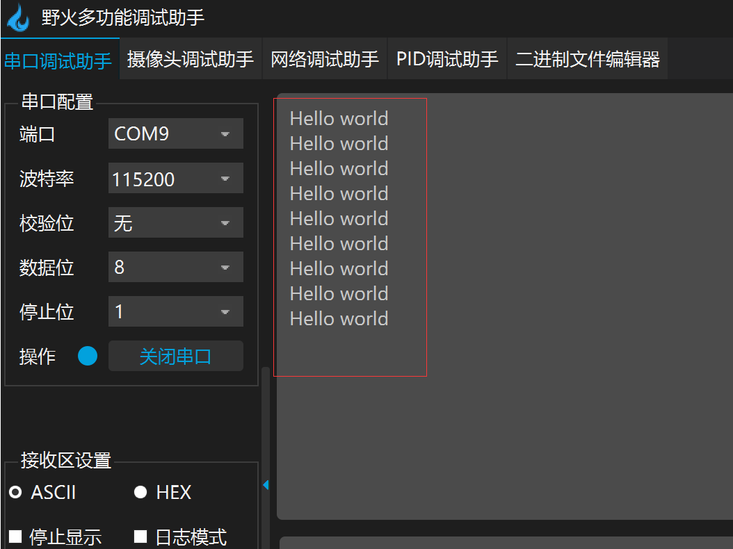
4. Serial port debugging
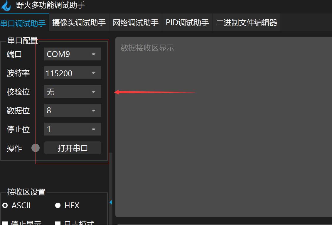
Operation results:
3, References
STM32 minimum core board F103 serial communication USART_ vic_ to_ CSDN blog
Creating STM32 assembler based on MDK: serial port output Hello world_ssj925319 blog - CSDN blog