brief introduction
This case is a simple oscilloscope based on the positive point atomic elite board, which can read the frequency and amplitude of the signal, and can change the sampling frequency and the update pause of the control screen by pressing the key. It's also adapted by learning from the experience of online tycoons. The following will introduce the basic principles used and the display of relevant codes.
A large part of it is to learn from this scheme (its code is register version):
Oscilloscope based on STM32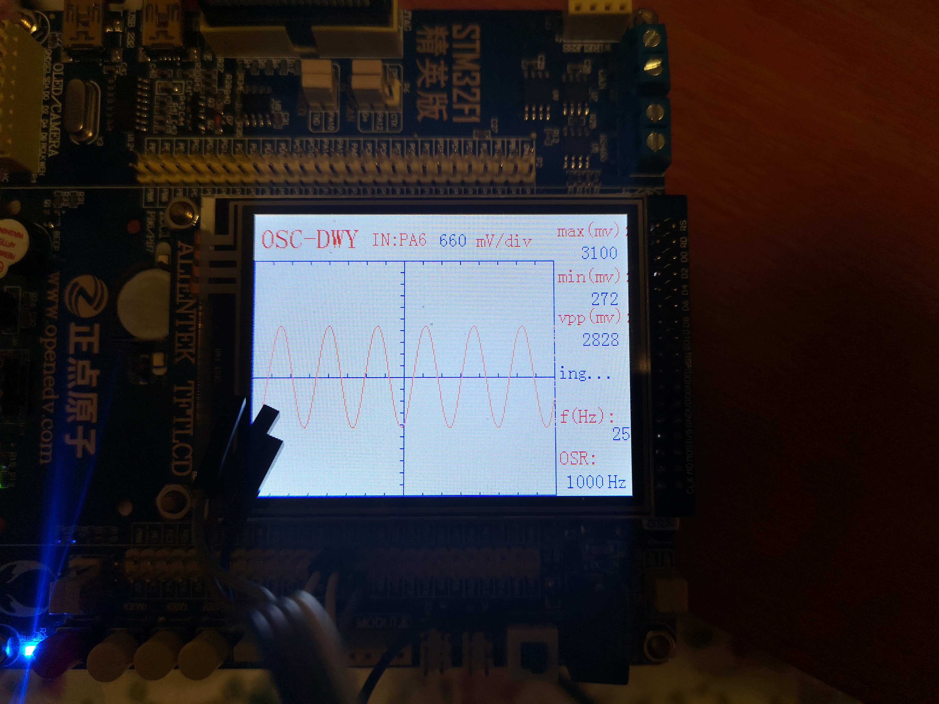
1, Signal acquisition
The signal acquisition mainly relies on ADC (trigger sampling by timer), and then stores the collected data into the cache array through DMA for subsequent data processing and waveform display. Through this method, the sampling rate can be accurately controlled.
In this case, channel 6 of ADC1 (PA6 port) is used for data sampling. It is necessary to change the trigger mode of ADC conversion to timer trigger (timer 2 is used for trigger). At the same time, when timer 2 is set to PWM mode, ADC can trigger sampling at each rising edge. Subsequently, the sampling frequency can be controlled by changing PWM frequency (i.e. prescaled value of timer).
A more specific explanation of the principle can be found in another big man:
[STM32] timer TIM triggers ADC sampling, DMA moves to memory (super detailed explanation)
1.ADC configuration:
void  Adc_Init(void)
{
	ADC_InitTypeDef ADC_InitStructure;
	GPIO_InitTypeDef GPIO_InitStructure;

	RCC_APB2PeriphClockCmd(RCC_APB2Periph_GPIOA |RCC_APB2Periph_ADC1, ENABLE );	  //Enable ADC1 channel clock


	RCC_ADCCLKConfig(RCC_PCLK2_Div6);   //Set ADC division factor 6 72M/6=12,ADC maximum time cannot exceed 14M

	//PA6 as analog channel input pin
	GPIO_InitStructure.GPIO_Pin = GPIO_Pin_6;
	GPIO_InitStructure.GPIO_Mode = GPIO_Mode_AIN;		//Analog input pin
	GPIO_InitStructure.GPIO_Speed = GPIO_Speed_50MHz;
	GPIO_Init(GPIOA, &GPIO_InitStructure);

	ADC_DeInit(ADC1);  //Reset ADC1, reset all registers of peripheral ADC1 to default value

	ADC_InitStructure.ADC_Mode = ADC_Mode_Independent;	//ADC working mode: ADC1 working in independent mode
	ADC_InitStructure.ADC_ScanConvMode = DISABLE;	//ADC works in single channel mode
	ADC_InitStructure.ADC_ContinuousConvMode = DISABLE;	//A / D conversion works in discontinuous conversion mode
	ADC_InitStructure.ADC_ExternalTrigConv = ADC_ExternalTrigConv_T2_CC2;	//The conversion is triggered by channel 2 of timer 2
	ADC_InitStructure.ADC_DataAlign = ADC_DataAlign_Right;	//ADC data right alignment
	ADC_InitStructure.ADC_NbrOfChannel = 1;	//The number of ADC channels in sequence for rule conversion
	ADC_Init(ADC1, &ADC_InitStructure);	//Initialize the registers of peripheral ADCx according to the parameters specified in ADC ﹣ initstruct


	ADC_Cmd(ADC1, ENABLE);	//Enable ADC1 specified

	ADC_DMACmd(ADC1, ENABLE);	//DMA function enable of ADC

	ADC_ResetCalibration(ADC1);	//Enable reset calibration

	ADC_RegularChannelConfig(ADC1, ADC_Channel_6, 1, ADC_SampleTime_1Cycles5 );//ADC1,ADC channel 6, sampling time 239.5 cycles

	ADC_ResetCalibration(ADC1);//Reset register

	while(ADC_GetResetCalibrationStatus(ADC1));	//Wait for reset calibration to finish

	ADC_StartCalibration(ADC1);	 //Enable AD calibration

	while(ADC_GetCalibrationStatus(ADC1));	 //Wait for calibration to finish

	ADC_SoftwareStartConvCmd(ADC1, ENABLE);		//Enable the specified ADC1 software conversion startup function

}
2. Timer configuration:
void TIM2_PWM_Init(u16 arr,u16 psc)
{
	GPIO_InitTypeDef GPIO_InitStructure;
	TIM_TimeBaseInitTypeDef  TIM_TimeBaseStructure;
	TIM_OCInitTypeDef  TIM_OCInitStructure;

	RCC_APB1PeriphClockCmd(RCC_APB1Periph_TIM2, ENABLE);	//Enable timer 3 clock
 	RCC_APB2PeriphClockCmd(RCC_APB2Periph_GPIOA  | RCC_APB2Periph_AFIO, ENABLE);  //Enable GPIO peripheral and AFIO multiplexing function module clock

   //Set this pin as multiplexing output function, output PWM pulse waveform GPIOA.1 of TIM2 CH2
	GPIO_InitStructure.GPIO_Pin = GPIO_Pin_1; //TIM_CH2
	GPIO_InitStructure.GPIO_Mode = GPIO_Mode_AF_PP;  //Multiplexing push pull output
	GPIO_InitStructure.GPIO_Speed = GPIO_Speed_50MHz;
	GPIO_Init(GPIOA, &GPIO_InitStructure);//Initialize GPIO

   //Initialize TIM3
	TIM_TimeBaseStructure.TIM_Period = arr; //Sets the value of the automatic reload register cycle that is loaded active at the next update event
	TIM_TimeBaseStructure.TIM_Prescaler =psc; //Set the prescaled value used as the divisor of TIMx clock frequency
	TIM_TimeBaseStructure.TIM_ClockDivision = 0; //Set clock division: TDTs = tk_tim
	TIM_TimeBaseStructure.TIM_CounterMode = TIM_CounterMode_Up;  //TIM count up mode
	TIM_TimeBaseInit(TIM2, &TIM_TimeBaseStructure); //Initializes the time base unit of TIMx based on the parameters specified in Tim ﹣ timebaseinitstruct

	//Initialize TIM3 Channel2 PWM mode
	TIM_OCInitStructure.TIM_OCMode = TIM_OCMode_PWM1; //Select timer mode: TIM PWM mode 2
 	TIM_OCInitStructure.TIM_OutputState = TIM_OutputState_Enable; //Compare output enable
	TIM_OCInitStructure.TIM_OCPolarity = TIM_OCPolarity_Low; //Output polarity: TIM output has high polarity
	TIM_OCInitStructure.TIM_Pulse=1000;
	TIM_OC2Init(TIM2, &TIM_OCInitStructure);  //Initialize peripheral TIM3 OC2 according to the parameters specified by T

	TIM_CtrlPWMOutputs(TIM2, ENABLE);
	TIM_Cmd(TIM2, ENABLE);  //Enabling TIM2
}
3.DMA configuration:
void MYDMA_Config(DMA_Channel_TypeDef* DMA_CHx,u32 cpar,u32 cmar,u16 cndtr)
{
	DMA_InitTypeDef DMA_InitStructure;
	NVIC_InitTypeDef NVIC_InitStructure;

 	RCC_AHBPeriphClockCmd(RCC_AHBPeriph_DMA1, ENABLE);	//Enable DMA transfer

    DMA_DeInit(DMA_CHx);   //Reset DMA channel 1 register to default
	DMA_InitStructure.DMA_PeripheralBaseAddr = cpar;  //DMA peripheral ADC base address
	DMA_InitStructure.DMA_MemoryBaseAddr = cmar;  //DMA memory base address
	DMA_InitStructure.DMA_DIR = DMA_DIR_PeripheralSRC;  //Data transmission direction, read from peripheral and send to memory//
	DMA_InitStructure.DMA_BufferSize = cndtr;  //DMA cache size for DMA channels
	DMA_InitStructure.DMA_PeripheralInc = DMA_PeripheralInc_Disable;  //Peripheral address register unchanged
	DMA_InitStructure.DMA_MemoryInc = DMA_MemoryInc_Enable;  //Memory address register increment
	DMA_InitStructure.DMA_PeripheralDataSize = DMA_PeripheralDataSize_HalfWord;  //Data width is 16 bits
	DMA_InitStructure.DMA_MemoryDataSize = DMA_MemoryDataSize_HalfWord; //Data width is 16 bits
	DMA_InitStructure.DMA_Mode = DMA_Mode_Circular;  //Working in cycle mode
	DMA_InitStructure.DMA_Priority = DMA_Priority_High; //DMA channel x has high priority
	DMA_InitStructure.DMA_M2M = DMA_M2M_Disable;  //DMA channel x is not set to memory to memory transfer
	DMA_Init(DMA_CHx, &DMA_InitStructure);  //ADC1 matches DMA channel 1

	DMA_ITConfig(DMA1_Channel1,DMA1_IT_TC1,ENABLE);	//Enable DMA transfer interrupt


	//Configure interrupt priority
	NVIC_InitStructure.NVIC_IRQChannel = DMA1_Channel1_IRQn;
	NVIC_InitStructure.NVIC_IRQChannelPreemptionPriority=0 ;
	NVIC_InitStructure.NVIC_IRQChannelSubPriority = 0;
	NVIC_InitStructure.NVIC_IRQChannelCmd = ENABLE;
	NVIC_Init(&NVIC_InitStructure);

	DMA_Cmd(DMA1_Channel1,ENABLE);//Enable DMA channel
}
2, Data processing
Data processing is mainly to obtain the frequency and amplitude of the signal and other related parameters. The amplitude can be obtained by the data collected by ADC through regression processing. The difficulty mainly lies in the acquisition of frequency. A signal may contain multiple frequency components, and what I display is the frequency component with the largest amplitude (of course, other frequencies can also be obtained). Here we use FFT (fast Fourier transform) in the DSP library function provided by STM32. As for the detailed conversion principle, it has not been fully understood.
Detailed information can be used for reference:
How to use DSP library for FFT
Function to get frequency:
#define NPT 1024//Sampling points of a complete collection

void GetPowerMag(void)
{
    float X,Y,Mag,magmax;//Real part, imaginary part, frequency amplitude, maximum amplitude
    u16 i;

	//Provided in DSP library, this function needs to collect 1024 points for processing
	cr4_fft_1024_stm32(fftout, fftin, NPT);

    for(i=1; i<NPT/2; i++)
    {
		X = (fftout[i] << 16) >> 16;
		Y = (fftout[i] >> 16);

		Mag = sqrt(X * X + Y * Y);
		FFT_Mag[i]=Mag;//It can be used for serial port output check

		//Obtain the maximum frequency component and its amplitude
		if(Mag > magmax)
		{
			magmax = Mag;
			temp = i;
		}
    }
	F=(u16)(temp/(pre/36.0));//pre is the prescaled value of timer 2. The modified formula is derived from the output result and the actual value. The specific principle has not been clarified
	LCD_ShowNum(280,180,F,5,16);
}
3, Analog sine wave output
This item mainly uses DAC output to constantly change the output value of DAC in the interrupt of timer 3, and generate a sine wave. Therefore, changing the frequency of sine wave can be achieved by changing the overflow time (reload value and prescaled value) of timer 3.
Here is the code:
u16 magout[NPT];
//Sine wave initialization value, before when (1).
//The output of sine wave is 0~3.3V, which is equivalent to an AC / DC flow. Because negative values cannot be sampled directly
void InitBufInArray(void)
{
    u16 i;
    float fx;
    for(i=0; i<NPT; i++)
    {
        fx = sin((PI2*i)/NPT);
        magout[i] = (u16)(2048+2048*fx);
    }
}

//Sine wave output, put this function in the interrupt of timer 3
void sinout(void)
{
	static u16 i=0;
	DAC_SetChannel1Data(DAC_Align_12b_R,magout[i]);
	i++;
	if(i>=NPT)
		i=0;
}
4, Other display and key control, etc
1. To display the waveform, only select a part of the obtained 1024 sampling data for display
The general idea is as follows:
u16 pre_vol;//Ordinate of corresponding point of current voltage value
u16 past_vol;//Ordinate of the point corresponding to the previous voltage value
//adcx [] array and 1024 raw data stored by DMA
pre_vol = 50+adcx[x]/4096.0*100;
LCD_DrawLine(x,past_vol,x+1,pre_vol);//According to the actual situation, the marking position can be changed accordingly
past_vol = pre_vol;
2. The key is controlled in the external interrupt (the corresponding reference code is provided in the punctual atom data)
It is more important to change the sampling frequency.
The prescalerconfig (Tim? Typedef * timx, uint16? Prescaler, uint16? Tim? Pscroloadmode) function can be used to change the prescaler value of timer 2.
The first time I wrote an article, I wrote so many first, many places need to be improved, and the code has some defects. I hope to communicate with you and learn from each other.

