S3C2440A clock system
This paper is based on the learning notes of weidongshan video
Clock system
OVERVIEW
The Clock & Power management block consists of three parts: Clock control, USB control, and Power control.
The Clock control logic in S3C2440A can generate the required clock signals including FCLK for CPU, HCLK for the AHB bus peripherals, and PCLK for the APB bus peripherals.
2440A can generate three clocks:
- FCLK of CPU
- HCLK of AHB bus (Advanced High performance Bus)
- PCLK of APB bus
The S3C2440A has two Phase Locked Loops (PLLs): one for FCLK, HCLK, and PCLK, and the other dedicated for USB block (48Mhz). The clock control logic can make slow clocks without PLL and connect/disconnect the clock to each peripheral block by software, which will reduce the power consumption.
2440A has two PLLs, one for FCLK, HCLK and PCLK, and the other for USB module (48Mhz).
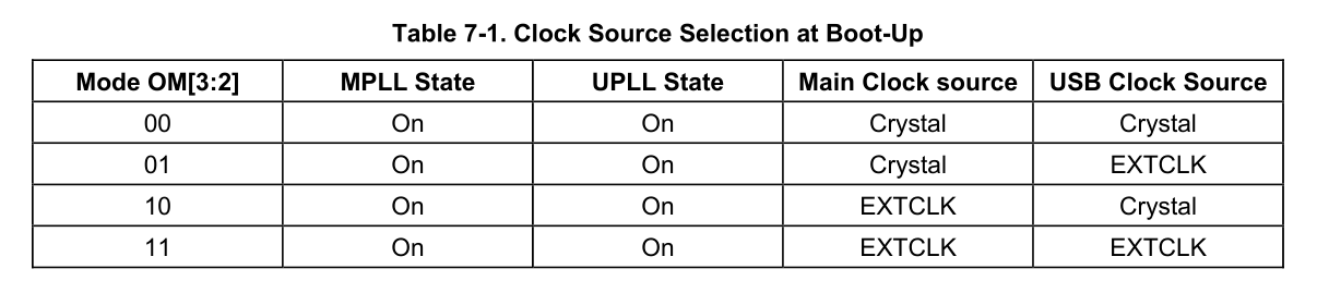
The figure above shows how to select the clock source. However, OM[3:2] is the first one by default, because in the hardware schematic diagram, both pins are grounded.
NOTES:
- Although the MPLL starts just after a reset, the MPLL output (Mpll) is not used as the system clock until the software writes valid settings to the MPLLCON register. Before this valid setting, the clock from external crystal or EXTCLK source will be used as the system clock directly. Even if the user does not want to change the default value of MPLLCON register, the user should write the same value into MPLLCON register.
- OM[3:2] is used to determine a test mode when OM[1:0] is 11.
In the last sentence of the first paragraph, we get a very important message: whether users want to change the default configuration or not, they need to write data for MPLLCON register. We got the first key clue: MPLLCON register must be configured.
The next part of the document is the introduction of PLL, skipping first.
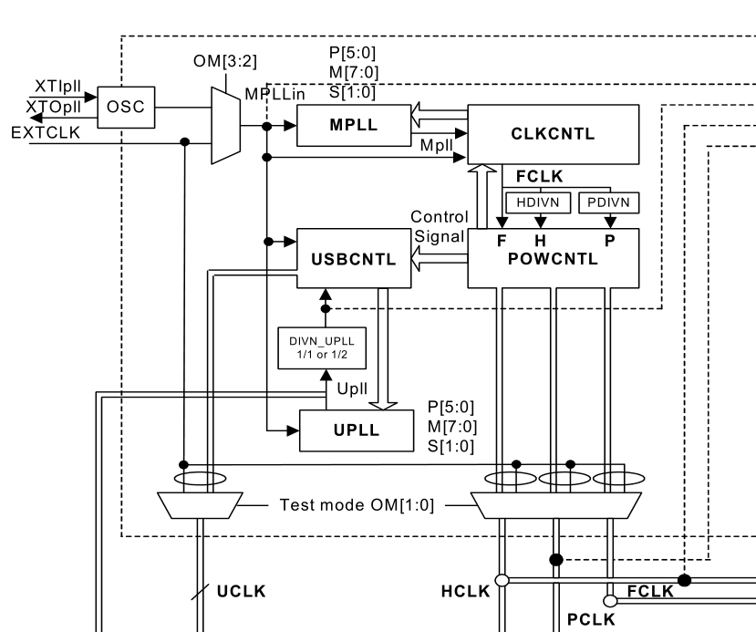
Turn down to clock control logic, which is important.
The Clock Control Logic determines the clock source to be used, i.e., the PLL clock (Mpll) or the direct external clock (XTIpll or EXTCLK). When PLL is configured to a new frequency value, the clock control logic disables the
FCLK until the PLL output is stabilized using the PLL locking time. The clock control logic is also activated at power-on reset and wakeup from power-down mode.
When PLL is configured, FLCK will stop until it is configured and stable.
Power-On Reset (XTIpll)
Figure 7-4 shows the clock behavior during the power-on reset sequence. The crystal oscillator begins oscillation within several milliseconds. When nRESET is released after the stabilization of OSC (XTIpll) clock, the PLL starts to operate according to the default PLL configuration. However, PLL is commonly known to be unstable after power-on reset, so Fin is fed directly to FCLK instead of the Mpll (PLL output) before the software newly configures the PLLCON. Even if the user does not want to change the default value of PLLCON register after reset, the user should write the same value into PLLCON register by software.
Here's another important message. When nRESET reset is released and stabilized, PLL is initially the default configuration.
But!!!
PLL is very unstable when it is powered on, so when the software reconfigures PLLCON, the Fin signals are sent directly to FCLK, that is to say, there is no PLL without configuration.
So whether the user wants to change the default configuration or not, they need to write data for PLLCON register. Here's the first clue.
The PLL restarts the lockup sequence toward the new frequency only after the software configures the PLL with a new frequency. FCLK can be configured as PLL output (Mpll) immediately after lock time.
Here, when PLL is configured, there will be a lock time.
Turn down again, and skip the USB bus first.
FCLK is used by ARM920T.
HCLK is used for AHB bus, which is used by the ARM920T, the memory controller, the interrupt controller, the LCD controller, the DMA and USB host block.
PCLK is used for APB bus, which is used by the peripherals such as WDT, IIS, I2C, PWM timer, MMC interface, ADC, UART, GPIO, RTC and SPI.
The S3C2440A supports selection of Dividing Ratio between FCLK, HLCK and PCLK. This ratio is determined by HDIVN and PDIVN of CLKDIVN control register.
There is a division ratio among fclk, hclk and PCLK, which is determined by HDIVN and PDIVN in CLKDIVN.
NOTES
- CLKDIVN should be set carefully not to exceed the limit of HCLK and PCLK.
- If HDIVN is not 0, the CPU bus mode has to be changed from the fast bus mode to the asynchronous bus mode using following instructions(S3C2440 does not support synchronous bus mode).
MMU_SetAsyncBusMode
mrc p15,0,r0,c1,c0,0
orr r0,r0,#R1_nF:OR:R1_iA
mcr p15,0,r0,c1,c0,0
If HDIVN is not 0 and the CPU bus mode is the fast bus mode, the CPU will operate by the HCLK.
This feature can be used to change the CPU frequency as a half or more without affecting the HCLK and PCLK.
Here is another important message: if HDIVN is not 0, the following instructions must be used to change the CPU bus mode from fast bus mode to asynchronous bus mode (S3C2440 does not support synchronous bus mode).
Now let's sort it out
We want the clock system to run normally. First, the configuration of MPLLCON. Second, set the division ratio of HDIVN and PDIVN. Third, set the asynchronous bus mode.
Look back at Figure 7-1 of the document
- OSC crystal oscillator or external crystal oscillator generates signal source, which is determined by the setting of OM[3:2].
- Configure MPLL and set the frequency of FCLK
- Configure HDIVN and set the frequency of HCLK
- Configure PDIVN and set PCLK frequency
Configure three clocks of 2440A, that's all
register
How to configure such parameters
- FCLK 400MHz
- HCLK 100MHz
- PCLK 50MHz
In fact, it's also simple. All the items that need to be configured have been bold in the font above. For the configuration of MPLLCON, the document gives the formula:
MPLL Control Register
Mpll = (2 * m * Fin) / (p * 2 S )
m = (MDIV + 8), p = (PDIV + 2), s = SDIV
This is the frequency calculation method of FCLK, but because it is too complex, the document also gives reference parameters.
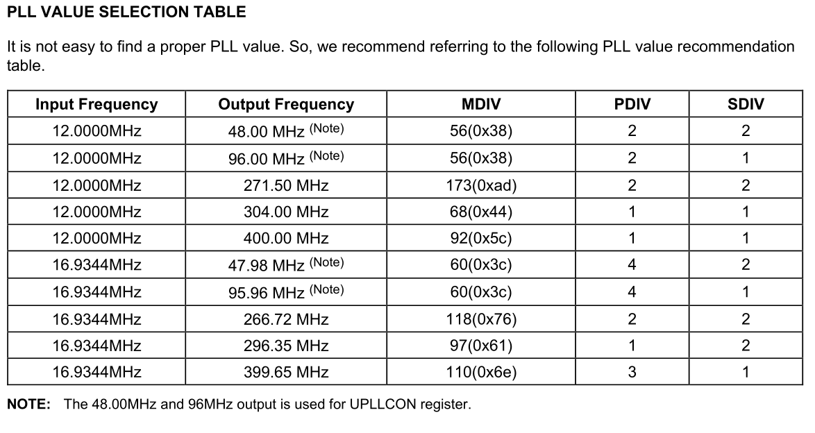
That is, set MDIV to 92(0X5C) and PDIV SDIV to 1.
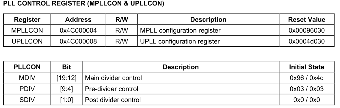
Look at this PLLCON register
PLLCON register address: 0x4C000004
MDIV [19:12] : 0x5C
PDIV [9:4] : 1
SDIV [1:0] : 1
That is: [0x4c000004] = 0b101 11000000 0001 0001 = 0x5C011
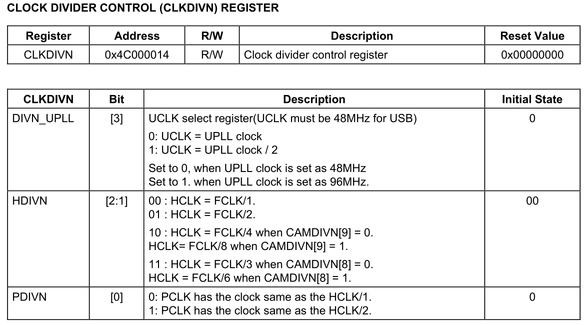
Look at the CLKDIVN register again
To make FCLK:HCLK:PCLK = 1:4:8
Picture understanding
CLKDIVN register address: 0x4C000014
HDIVN [2:1] : 0b10
PDIVN [0] : 0b1
That is: [0x4C000014] = 0b101 = 0x5
At this point, the two registers are set, and finally set to asynchronous mode.
Modify the code led.S on the basis of the flow light in the previous lesson
.text
.global _start

_start:

	/* Close the watchdog */
	ldr r0, =0x53000000
	ldr r1, =0
	str r1, [r0]  /* Set the zero position of WTCON to 0 and close the watchdog */

	/* Set PLLCON to FLCK = 400MHz
	 * PLLCON Register address: 0x4C000004
	 * MDIV  [19:12] : 0x5C
	 * PDIV [9:4]	 : 1
	 * SDIV [1:0]    : 1
	 * That is: [0x4c000004] = 0b101 11000000 0001 0001 = 0x5C011
	 */
	mov r0, 0x4C000004
	mov r1, 0x5C011
	mov [r0], r1

	/* Set the CLKDIVN register so that FCLK:HCLK:PCLK = 1:4:8
	 * CLKDIVN Register address: 0x4C000014
	 * HDIVN [2:1] : 0b10
	 * PDIVN [0] : 0b1
	 * That is: [0x4C000014] = 0b101 = 0x5
	 */
	mov r0, 0x4C000014
	mov r1, 0x5
	mov [r0], r1

	/* Set sp stack to automatically identify whether nor or nand starts
	 * nor When starting, it corresponds to nor flash, and when nand starts, it corresponds to on-chip memory
	 * There must be a certain format when writing data in nor flash
	 * Write 0 to the 0 address, and read it again to see if there is any modification. If there is modification, it is nand startup, if there is no modification, it is nor startup
	 */

	ldr sp ,= 4096 /*nand start-up*/

	mov r1, #0
	ldr r0, [r1] /* First, back up the value of [0] address to r0 */
	str r1, [r1] /* Write 0 to [0] address */
	ldr r2, [r1] /* Read the value of [0] address again */
	cmp r1,r2    /* compare */
	ldr sp, =0x400000000+4096 /* nor start-up */
	moveq sp , #4096 /*nand start*/
	streq r0, [r1] /* Restore data */

	bl main

halt:
	b halt

