1. Introduction to PulseSensor
(1) Working principle
PulseSensor is a photoelectric reflective analog sensor for pulse and heart rate measurement. Wear it on the finger or earlobe, etc. through wire connection, the collected analog signal can be transmitted to stm32, Arduino and other MCU, and analog-to-digital conversion (voltage acquisition) can be carried out on the MCU. The heart rate value can be obtained after heart rate calculation. In addition, the ECG data can be uploaded to the computer to display the waveform. In this paper, STM32F103 series will be used to realize the above functions.
The workflow of PulseSensor is shown in the following figure:

(2) Performance parameters
The basic performance parameters of PulseSensor are as follows:
Circuit board diameter: 16mm
Thickness of circuit board: 1.6mm (thickness of ordinary PCB board)
LED peak wavelength: 515nm (green light)
Power supply voltage: 3.3V or 5V
Output signal type: analog signal
Output signal size: 0~3.3V(3.3V power supply) or 0~5V(5V power supply)
(3) Pin description
The back of PulseSensor is shown in the figure below:
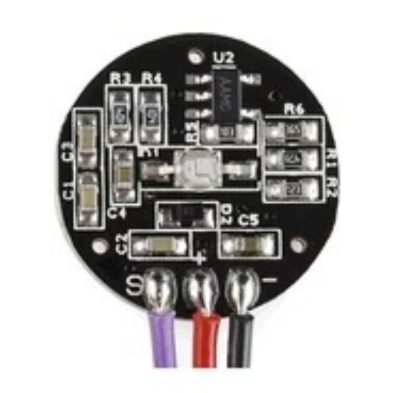
There are three leads under the circuit board, which are from left to right:
S: Singal, analog signal output, connected to GPIO pin on MCU (configured as analog input function for voltage acquisition)
+: the positive pole of the power supply is connected to the 5V pin or 3,3V pin of the single chip microcomputer
–: the negative pole of the power supply is connected to the GND pin of the single chip microcomputer
2. DMA configuration in PulseSensor development
(1) DMA introduction
DMA(Direct Memory Access) - direct memory access, which is a separate peripheral independent of the kernel in the single chip microcomputer. Its main function is to realize the fast transmission from memory to memory, memory to peripherals and peripherals to memory without occupying CPU.
When transmitting data to the memory through DMA, the DMA request must be sent to the DMA controller first. After DMA receives the request signal, the controller will send a response signal to the peripheral. When the peripheral responds and the DMA receives the response signal, it is good to enable DMA transmission until the transmission is completed.
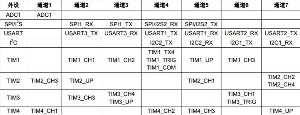
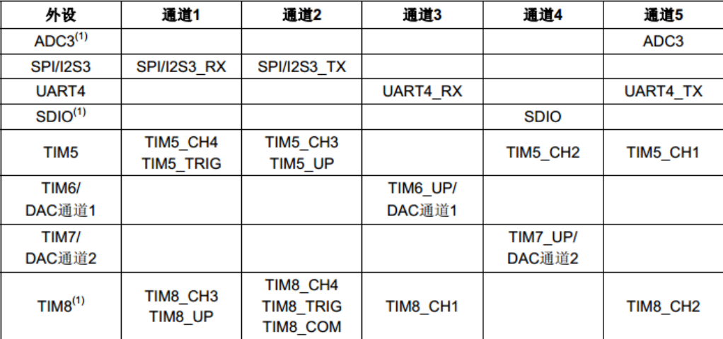
DMA has two controllers, DMA1 and DMA2. DMA1 has seven channels and DMA2 has five channels. The channels of different DMA controllers correspond to different peripheral requests. The specific image comparison is as follows:
Peripherals controlled by 7 peripheral channels of DMA1:
Peripherals controlled by 5 peripheral channels of DMA2:
(2) Considerations of DMA in PulseSensor development
1. Data transmission direction
DMA transfers data in three directions: from peripheral to memory, from memory to peripheral, and from memory to memory. In the development of PulseSensor, we set the DMA data transmission direction as * * from peripheral to memory. The peripheral here is the regular data register ADC1 of ADC_ Dr stores the converted ECG. The memory is an array ADC defined by itself_ ConvertValue[NUMCHANNEL]. ** When processing the output information, we only need to operate on the array ADC_ConvertValue []. Since ADC1 is enabled for voltage acquisition, it corresponds to channel 1 of DMA1. The peripheral address involved in this is determined by DMA_CPAR configuration, memory address is determined by DMA_CMAR configuration.
2. Unit of data transmitted
Since the acquisition accuracy of ADC is 12 bits, at least a 16 bit variable (array) should be used to store data in data reading processing. That is, the size of peripheral data should be two bytes (HalfWord). And in order to ensure correct data transmission, we also make the data width of the memory two bytes.
3. Address increment of peripheral and memory
The peripheral is the regular data register ADC1 of ADC_ Dr, there is only one register and the address remains unchanged. The memory is array ADC_ConvertValue [], when data is passed in at a certain position of the array, the next data will be passed in at the next position of the current array address. Therefore, the memory address should be kept increasing,
(3) Related configuration procedures of DMA in PulseSensor
/**NUMCHANNEL here is determined by the number of acquisition channels required by the actual demand*/
__IO uint16_t ADC_ConvertValue[NUMCHANNEL] = {0};

DMA_InitTypeDef DMA_InitStructure;
/**Turn on the clock of DMA and ADC. DMA is a high-performance module, and the AHB clock should be turned on as the clock driver of DMA*/
RCC_AHBPeriphClockCmd(ADC_DMA_CLK, ENABLE);
/**Reset the DMA channel configuration register to the default value*/
DMA_DeInit(ADC_DMA_CHANNEL);

/**The peripheral address is the regular data register ADC_DR*/
DMA_InitStructure.DMA_PeripheralBaseAddr = (u32)( & (ADC_x ->DR));
/**The memory address is ADC_ConvertValue*/
DMA_InitStructure.DMA_MemoryBaseAddr = (u32)ADC_ConvertValue;
/**The data reading direction is from the peripheral to the memory*/
DMA_InitStructure.DMA_DIR = DMA_DIR_PeripheralSRC;
/**The size of the data buffer is the size of the memory NUMCHANNEL*/
DMA_InitStructure.DMA_BufferSize = NUMCHANNEL;
/**Peripheral register ADC_ The Dr address value remains unchanged and the address does not need to be incremented*/
DMA_InitStructure.DMA_PeripheralInc = DMA_PeripheralInc_Disable;
/**Memory address increment*/
DMA_InitStructure.DMA_MemoryInc = DMA_MemoryInc_Enable;
/**The size of peripheral data is half word, that is, two bytes*/
DMA_InitStructure.DMA_PeripheralDataSize = DMA_PeripheralDataSize_HalfWord;
/**The memory data size is also half a word, which is the same as the peripheral data size*/
DMA_InitStructure.DMA_MemoryDataSize = DMA_MemoryDataSize_HalfWord;
/**Set the DMA working mode to the cyclic transmission mode, and the DMA operation will continue*/
DMA_InitStructure.DMA_Mode = DMA_Mode_Circular;
/**DMA Transmission channel priority is high*/
DMA_InitStructure.DMA_Priority = DMA_Priority_High;
/**The read data direction is from the peripheral to the memory, so the memory to memory mode is disabled*/
DMA_InitStructure.DMA_M2M = DMA_M2M_Disable;
/**Initialize DMA according to the above configuration*/
DMA_Init(ADC_DMA_CHANNEL, &DMA_InitStructure);
3. ADC configuration in PulseSensor development
(1) ADC introduction
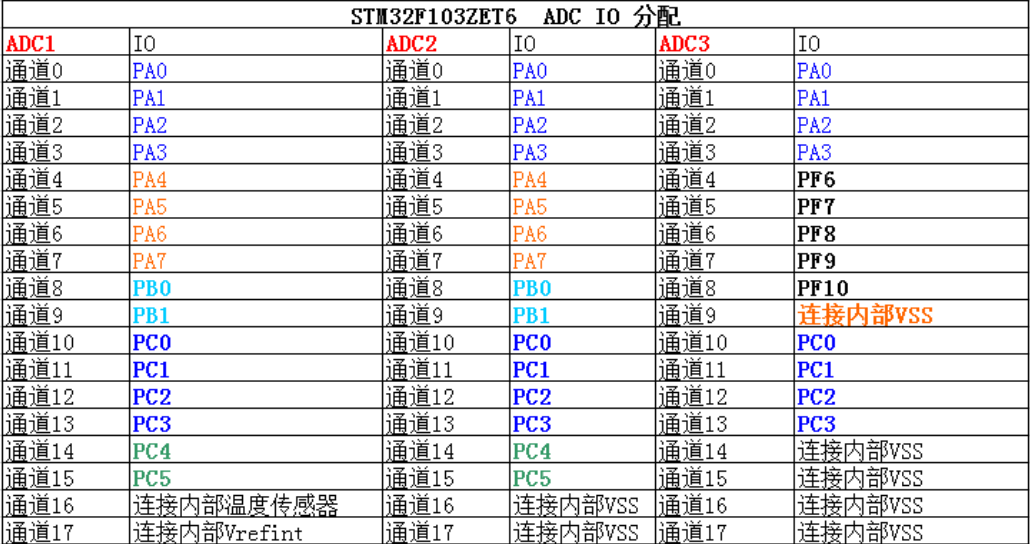
The full name of ADC is: analog to digital converter, which means analog-to-digital converter. STM32f103 series has 3 ADCs with 12 bit accuracy, and each ADC has up to 16 external channels. ADC1 and ADC2 have 16 external channels, and ADC3 has 8 external channels according to different CPU pins.
The voltage input range of ADC is 0 ~ 3.3V. If you want to broaden the input voltage range, you can connect a voltage conditioning circuit outside the input pin to raise or lower the voltage to be converted to the range of 0 ~ 3.3V. In this way, ADC can measure the corresponding voltage value. Then multiply the read voltage value by the adjustment coefficient (the ratio of input and output) of the voltage conditioning circuit.
The IO ports (peripherals) corresponding to the three ADC channels are shown in the figure below:
(2) Precautions of ADC in PulseSensor development
1. Conversion time and pin mode configuration
ADC input clock ADC_CLK is generated by PCLK2 through frequency division, and the maximum is 14M. The shortest sampling period is 1.5 cycles, that is, at least 0.11us. The conversion time of ADC is related to the input clock and sampling time of ADC. The formula is: T = sampling time + 12.5 cycles. When ADCLK = 14MHZ (highest) and the sampling time is set to 1.5 cycles (fastest), the total conversion time (shortest) Tmin = 1.5 cycles + 12.5 cycles = 14 cycles = 1US.
ADC voltage acquisition pin, GPIO operating mode must be configured as analog input. This mainly considers that the other three input configuration modes (floating input, pull-up input and pull-down input) clamp the input voltage at high level or low level, which will cause serious distortion of the signal. Only the analog input mode does not have any amplitude modulation for the input voltage.
2. Conversion end behavior
When the voltage conversion ends. ADC can remind the system of the end of conversion and read data in two ways** One is interrupt, * * and the interrupt trigger type is divided into regular channel conversion end interrupt, injection conversion channel conversion end interrupt and analog watchdog interrupt** The other is DMA request, which directly stores the converted data in memory. It should be noted that only ADC1 and ADC3 can generate DMA requests.
3. Voltage conversion
After ADC conversion, the analog voltage is a 12 bit digital value. If it is printed directly by serial port or processed directly, it will not only reduce the readability, but also reduce the readability and increase the difficulty of data processing. Therefore, we also need a set of conversion formula to convert the 12 bit digital value into the actual voltage. Considering the linear relationship between the digital value and the actual voltage value, and when the 12 bit full scale. The corresponding voltage is 3.3V. Such a conversion formula can be obtained for a long time:
Actual voltage value V = (3.3 * 12 digit measured value X)/ 2^12.
(3) Related configuration procedures of ADC in PulseSensor
/**
 *@brief     Initialize the configuration of voltage acquisition GPIO port
 *@attention The IO used for ADC acquisition must not be multiplexed by other peripherals, otherwise it will have a numerical impact on the acquisition voltage
 *@param     nothing
 *@retval    nothing
 */
static void ADCx_GPIO_Config(void)
{
	GPIO_InitTypeDef GPIO_InitStructure;
	/**Turn on GPIO port clock*/
	ADC_GPIO_APBxClock_Cmd(ADC_GPIO_CLK, ENABLE);
    GPIO_InitStructure.GPIO_Pin = ADC_PIN1 | ADC_PIN2;
	/**Set GPIO operating mode to analog input mode*/
	GPIO_InitStructure.GPIO_Mode = GPIO_Mode_AIN;
	GPIO_Init(ADC_PORT, &GPIO_InitStructure);

	GPIO_InitStructure.GPIO_Pin = ADC_PIN3 | ADC_PIN4 | ADC_PIN5 | ADC_PIN6;
	/**Set GPIO operating mode to analog input mode*/
	GPIO_InitStructure.GPIO_Mode = GPIO_Mode_AIN;
	GPIO_Init(ADC_PORT1, &GPIO_InitStructure);
}
ADC_InitTypeDef ADC_InitStructure;
/**Turn on the clock of ADC*/
ADC_APBxClock_Cmd(ADC_CLK, ENABLE);

/**Set the ADC operating mode to independent operating mode*/
ADC_InitStructure.ADC_Mode = ADC_Mode_Independent;
/**The scan mode is enabled in the multi-channel ADC voltage collector and disabled in the single channel voltage collector*/
ADC_InitStructure.ADC_ScanConvMode = ENABLE;
/**Turn on connection conversion mode*/
ADC_InitStructure.ADC_ContinuousConvMode = ENABLE;
/**No external trigger conversion is needed, and the mode of software startup is adopted*/
ADC_InitStructure.ADC_ExternalTrigConv = ADC_ExternalTrigConv_None;
/**Align conversion results right*/
ADC_InitStructure.ADC_DataAlign = ADC_DataAlign_Right;
/**The number of conversion channels is NUMCHANNEL*/
ADC_InitStructure.ADC_NbrOfChannel = NUMCHANNEL;
/**Initialize the ADC according to the above configuration*/
ADC_Init(ADC_x, &ADC_InitStructure);
/**Configure the ADC clock as 8 frequency division of PCLK2, i.e. 9MHZ*/
RCC_ADCCLKConfig(RCC_PCLK2_Div8);

/**Configure ADC channel conversion sequence and sampling time, where the sampling time is 55.5 cycles*/
ADC_RegularChannelConfig(ADC_x, ADC_CHANNEL1, 1, ADC_SampleTime_55Cycles5);
ADC_RegularChannelConfig(ADC_x, ADC_CHANNEL2, 2, ADC_SampleTime_55Cycles5);
ADC_RegularChannelConfig(ADC_x, ADC_CHANNEL3, 3, ADC_SampleTime_55Cycles5);
ADC_RegularChannelConfig(ADC_x, ADC_CHANNEL4, 4, ADC_SampleTime_55Cycles5);
ADC_RegularChannelConfig(ADC_x, ADC_CHANNEL5, 5, ADC_SampleTime_55Cycles5);
ADC_RegularChannelConfig(ADC_x, ADC_CHANNEL6, 6, ADC_SampleTime_55Cycles5);

/**Enable DMA direct memory reading without enabling interrupt*/
ADC_DMACmd(ADC_x, ENABLE);
/**Enable ADC1*/
ADC_Cmd(ADC_x, ENABLE);
/**Turn on the ADC and start the conversion*/
ADC_ResetCalibration(ADC_x);
/**Wait for the reset to complete*/
while(ADC_GetResetCalibrationStatus(ADC_x));
/**Starts the calibration process for the selected ADC*/
ADC_StartCalibration(ADC_x);
/**Wait for calibration to complete*/
while(ADC_GetCalibrationStatus(ADC_x));
/**Enable ADC software triggered conversion*/
ADC_SoftwareStartConvCmd(ADC_x, ENABLE);
4. Main function data acquisition and output
After DMA and ADC are configured, you only need to initialize once in the main function to read the array ADC_ConvertValue [] to get ECG value at any time.
(1) Main function program
int main(void)
{
	int a1, a2, a3, a4;
	/**Initialize Usart*/
	Usart_Config();
	/**Initialize ADC and DMA configuration*/
	ADCx_Init();
	/**Initialize the basic timer TIM3 and configure it to generate a timer interrupt every 1ms*/
	CURRENT_TIM_Init();
	while(1)
	{
		/**20ms Send a data*/
		if(tim3_count >= 20)
		{
			/**The voltage can be collected in BSP according to the actual needs_ Change pin in ADC. H*/
		  ADC_ConvertValueLocal[2] = (int16_t)ADC_ConvertValue[2];
			/**Bit splitting is for the upper function to receive data normally, and can also be sent directly according to actual needs*/
		  a1 = ADC_ConvertValueLocal[2] / 1000;
		  a2 = ADC_ConvertValueLocal[2] % 1000 / 100;
		  a3 = ADC_ConvertValueLocal[2] % 1000 % 100 / 10;
		  a4 = ADC_ConvertValueLocal[2] % 1000 % 100 % 10;
		  printf("AAA%d%d%d%d", a1, a2, a3, a4);
		  tim3_count = 0;
		}
	}
}
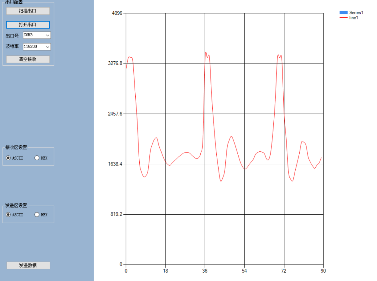
(2) Upper computer waveform display
Upload the data to the upper computer and view it in the self-made upper computer software:
5. Summary
The data acquisition part of PulseSensor is relatively simple, but the reading of sensor data is only the first step. The analysis of sensor waveform data, the calculation of heart rate and even the design of host computer are the more critical parts, which will be involved in the subsequent development documents.