NXP SJA1124 spi to lin chip driver
1, Overall characteristics
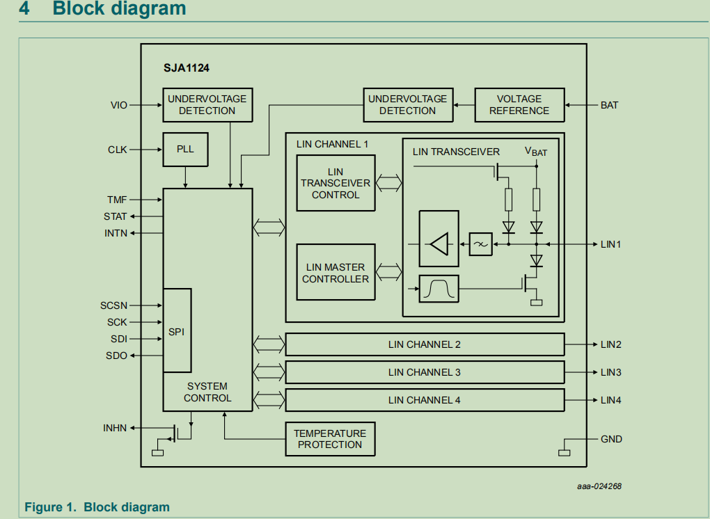
1.sja1124 is an integrated chip of lin controller and transceiver, which supports four lin channels.
2. Support LIN 2.0, LIN 2.1, LIN 2.2, LIN 2.2A and relevant international protocol standards, and can reach 20kb baud rate at the fastest
3. Wake up in low power mode through spi or lin
4. An external clock is required as the lin communication clock source.
5. For hardware lin communication, only the registers need to be configured.
6. Structural frame diagram
2, Working mode
1. The five modes of the chip are shown in the figure below. Note that the manual is divided into chip mode and lin mode, and there will be modes with duplicate names. If lin mode is involved, lin will be added, otherwise it is generally chip mode.
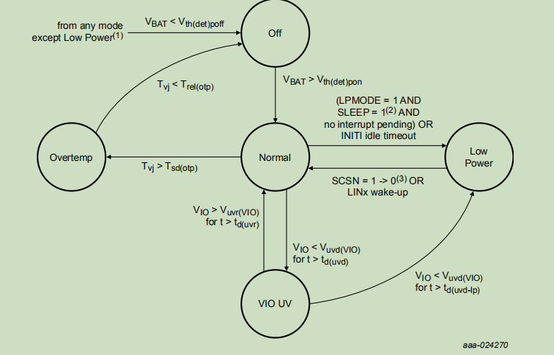
2. After the chip is powered on, there will be an INITI idie timeout of 3.2s. Without spi communication or lin wake-up at this time, the chip enters the low power mode.
3.lin modes include lin sleep, lin normal and lin initial. These are lin modes, such as initialization mode. If you use several lin channels, each lin channel needs to be initialized separately.
3, spi communication
spi communication is an 8-bit register. Generally, the communication with muc should pay attention to the following points. Of course, the specific spi communication should be learned from other people's articles, not the core of this article. This time I use NXP automotive MCU chip.
1. Clock frequency configuration bit communication frequency involves baud rate configuration
  /* DBR =0  BR=8   PBR=5   FP=40MHZ   BUAD= (40/5)*[(1+0)/8]=1M*/
SPI_2.MODE.CTAR[0].B.PBR=0b10;
SPI_2.MODE.CTAR[0].B.BR=0b0011;
2. Register configuration of transmission data bits. For example, the default 16 bit transmission data bits I use are generally 16 bits, and FMSZ needs to be set to 8 bits
	/*frame size*/
SPI_2.MODE.CTAR[0].B.FMSZ=0b0111;
3. The clock polarity and phase should be consistent with the high side chip. The clock polarity and phase of SJA1124 are divided into 0 and 1 respectively
SPI_2.MODE.CTAR[0].B.CPOL=0;   	//lin chip polarity and phase 0 1
SPI_2.MODE.CTAR[0].B.CPHA=1;
4. Read and write the pseudo code of the function
u8 FUN_HW_SJA1124_ReadData(u8 address)
{
	u8 data;

	HW_SJA1124_CS1=0;
	FUN_HW_Time_Delayus(1);
	SPI3_SendAndGetData_byte(address,HW_SJA1124_CS1);
	SPI3_SendAndGetData_byte(SJA1124READ,HW_SJA1124_CS1);		//Read 8-bit long data
	data=SPI3_SendAndGetData_byte(address,HW_SJA1124_CS1);
	FUN_HW_Time_Delayus(1);
	HW_SJA1124_CS1=1;

	return data;
}
void FUN_HW_SJA1124_WriteData(u8 address,u8 data)
{

	HW_SJA1124_CS1=0;
	FUN_HW_Time_Delayus(1);
	SPI3_SendAndGetData_byte(address,HW_SJA1124_CS1);
	SPI3_SendAndGetData_byte(SJA1124WRITE,HW_SJA1124_CS1);		//Read 8-bit long data
	SPI3_SendAndGetData_byte(data,HW_SJA1124_CS1);
	FUN_HW_Time_Delayus(1);
	HW_SJA1124_CS1=1;

}
3, lin communication
1. Communication is divided into master and slave. This time, the chip lin can only be used as the master. Briefly describe the lin communication protocol. For specific communication learning, you still have to read professional articles, which is not the focus of this time. This lin communication is a hardware lin and does not need software to simulate the communication protocol.
2.lin communication is mainly divided into two parts: header and response, as shown in the figure below
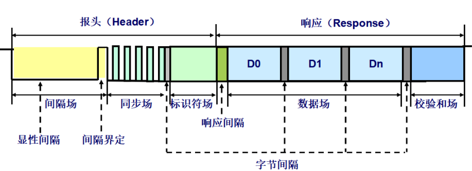
3.lin logic level is divided into explicit (0) and implicit (1). lin is a master-slave communication mode. Generally, there can be up to 16 slave nodes. In the communication process, the host must first send the header, then the slave response, the host is in the response, and then the infinite response.
4. The header has interval field, synchronization field and identifier field respectively. The interval field is generally greater than 13 dominant level bit s, while the synchronization field is fixed as "0x55" a byte, and the identifier is the PID of the sending header. The PID can be divided into ID and parity. The ID range is 0-0x3f, that is, 64. However, many special IDS cannot be used, and the parity here has special verification algorithms that can be used to check the table.
5. The response field is divided into data field and checksum field. The data field can be 2 / 4 / 8 bytes, generally 8 bytes, which is similar to can. The checksum field is the inverse code of the sum of all bytes in the data field. Now it is generally divided into classic and enhanced.
4, Chip register configuration
1. The register is the same as the mode, i.e. chip register and lin register respectively.
2. First, initialize the chip configuration register, involving IO, working mode and clock interrupt register configuration.
void FUN_HW_SJA1124_Init(void)
{
	//Pin initialization
	SIUL2.MSCR[PC15].B.SSS = 0;			/* Pin functionality as GPIO */
	SIUL2.MSCR[PC15].B.OBE = 1;          /* Output Buffer Enable off */
	SIUL2.MSCR[PC15].B.IBE = 0;			/* Input Buffer Enable on */
	/*clk*/
	SIUL2.MSCR[PB6].B.SSS = 1;			/* Pin functionality as GPIO */
	SIUL2.MSCR[PB6].B.OBE = 1;          /* Output Buffer Enable off */

	/*Mode selection*/
	SJA1124.MODE_reg.B.RST=1;//reset
	SJA1124.MODE_reg.B.LPMODE=0;    //0. Normal mode 1. Low power consumption
	FUN_HW_SJA1124_WriteData(SJA1124MODE,SJA1124.MODE_reg.R);
	/*Clock frequency setting*/
	SJA1124.PLLCFG_reg.B.PLLMULT=0X8;//  CLK=32M
	FUN_HW_SJA1124_WriteData(PLLCFG,SJA1124.PLLCFG_reg.R);
	//Wake up WUIE interrupt is enabled by default
	//Turn on all interrupts
	SJA1124.INT1EN_reg.R=0x0F;
	FUN_HW_SJA1124_WriteData(INT1EN,SJA1124.INT1EN_reg.R);
	SJA1124.INT2EN_reg.R=0x3E;
	FUN_HW_SJA1124_WriteData(INT2EN,SJA1124.INT2EN_reg.R);
	SJA1124.INT3EN_reg.R=0xFF;
	FUN_HW_SJA1124_WriteData(INT3EN,SJA1124.INT3EN_reg.R);
}
3. To initialize the Lin channel, the corresponding registers must be configured in INIT=1, that is, the Lin initialization mode. The main contents are the inspection method of Lin communication, interval length, related register configuration, baud rate and interrupt.
void FUN_HW_SJA1124_LIN1Init(void)
{

	/*LIN1 configuration */
	SJA1124.LCFG1_reg[0].B.CCD=0;//Hardware verification
	SJA1124.LCFG1_reg[0].B.MBL=0X3;//break dominant level length 16 bit - > 13 bit official demo
	SJA1124.LCFG1_reg[0].B.SLEEP=0;//Normal mode
	SJA1124.LCFG1_reg[0].B.INIT=1;//The initialization mode configuration must be in the initialization mode again
	FUN_HW_SJA1124_WriteData(LCFG1LIN1,SJA1124.LCFG1_reg[0].R);
	/*2-bit delimiter*/
	SJA1124.LCFG2_reg[0].B.TBDE=1;
	SJA1124.LCFG2_reg[0].B.IOBE=1;
	FUN_HW_SJA1124_WriteData(LCFG2LIN1,SJA1124.LCFG2_reg[0].R);

	/*idle on timeout*/
	SJA1124.LITC_reg[0].B.IOT=1;
	FUN_HW_SJA1124_WriteData(LITCLIN1,SJA1124.LITC_reg[0].R);
	/*2 stop bit congfiguraton*/
	SJA1124.LGC_reg[0].B.STOP=1;
	FUN_HW_SJA1124_WriteData(LGCLIN1,SJA1124.LGC_reg[0].R);
	/*response time*/
	SJA1124.LRTC_reg[0].R=0X0E;//The response time is to be determined. The recommended value is set
	FUN_HW_SJA1124_WriteData(LRTCLIN1,SJA1124.LRTC_reg[0].R);

	/*baud rate  If CLK is 16M */
	SJA1124.LFR_reg[0].B.FBR=0X2;//Set to 3
	FUN_HW_SJA1124_WriteData(LFRLIN1,SJA1124.LFR_reg[0].R);
	SJA1124.LBRM_reg[0].B.IBR=0X00;//No high position
	FUN_HW_SJA1124_WriteData(LBRMLIN1,SJA1124.LBRM_reg[0].R);
	SJA1124.LBRL_reg[0].B.IBR=LIN1BAUD;//Low position 104 * 16 + 3 = 1667 32m / 1667 = 19200;
	FUN_HW_SJA1124_WriteData(LBRLLIN1,SJA1124.LBRL_reg[0].R);

	SJA1124.LCFG1_reg[0].B.INIT=0;//Set back to normal mode
	FUN_HW_SJA1124_WriteData(LCFG1LIN1,SJA1124.LCFG1_reg[0].R);
	/*interrupt */
	FUN_HW_SJA1124_WriteData(LIELIN1,0xF7);//Enable all interrupts
}
4. Next is the setting of lin communication, including ID and data.
void FUN_HW_SJA1124_LIN1SendFrame( Lin1_PduType* LIN1Frame)
{
	//
	SJA1124.LC_reg[0].B.HTRQ=1;
	FUN_HW_SJA1124_WriteData(LIN1LC,SJA1124.LC_reg[0].R);
//	SJA1124.LCOM2_reg.B.L1HTRQ=1;
//	FUN_HW_SJA1124_WriteData(LIN1LC,SJA1124.LCOM2_reg.R);
	SJA1124.LBI_reg[0].B.ID=LIN1Frame->lin1id;//ID identifier setting range 0-0x3f
	FUN_HW_SJA1124_WriteData(LIN1LBI,SJA1124.LBI_reg[0].R);
	SJA1124.LINLBC_reg[0].B.DFL=LIN1Frame->lin1dfl;//Number of bytes DFL=value-1
	SJA1124.LINLBC_reg[0].B.DIR=LIN1Frame->lin1dir;//
	SJA1124.LINLBC_reg[0].B.CCS=LIN1Frame->lin1ccs;//0 is lin2.0 enhanced verification version 1 is lin1.3
	FUN_HW_SJA1124_WriteData(LIN1LBC,SJA1124.LINLBC_reg[0].R);


	/*tx data*/
	FUN_HW_SJA1124_WriteData(LIN1LDB1,LIN1Frame->lin1data[0]);
	FUN_HW_SJA1124_WriteData(LIN1LDB2,LIN1Frame->lin1data[1]);
	FUN_HW_SJA1124_WriteData(LIN1LDB3,LIN1Frame->lin1data[2]);
	FUN_HW_SJA1124_WriteData(LIN1LDB4,LIN1Frame->lin1data[3]);
	FUN_HW_SJA1124_WriteData(LIN1LDB5,LIN1Frame->lin1data[4]);
	FUN_HW_SJA1124_WriteData(LIN1LDB6,LIN1Frame->lin1data[5]);
	FUN_HW_SJA1124_WriteData(LIN1LDB7,LIN1Frame->lin1data[6]);
	FUN_HW_SJA1124_WriteData(LIN1LDB8,LIN1Frame->lin1data[7]);


	SJA1124.LS_tag[0].R=FUN_HW_SJA1124_ReadData(LIN1STATU);

}
5. Design the structure of header and response, and put the communication function into the structure.
typedef struct
{
  /* LBI register. */
  uint8_t lin1id;                /* LIN frame identifier. */
  /* LBC register. */
  uint8_t lin1dfl;               /* Data field length (number of bytes - 1). */
  Lin_FrameResponseType lin1dir; /* Response type (master or slave response). */
  Lin_FrameCsModelType lin1ccs;  /* Checksum model type (classic or enhanced checksum calculation). */
  /* LCF register. */
  uint8_t lin1cf;                /* Checksum to be transmitted in case checksum calculation is disabled. */
  /* LBDx registers. */
  uint8_t lin1data[8];           /* Pointer to data to send. */
} Lin1_PduType;
/* LIN1 Frame configuration. */
Lin1_PduType Frame1 = {
  .lin1id = 0x20,                /* Identifier - ID. */
  .lin1dfl = 7,                  /* Data field length = number of data bytes - 1. */
  .lin1dir = LIN_MASTER_RESPONSE, /* Direction - master to slave. */
  .lin1ccs = LIN_ENHANCED_CS,     /* Enhanced checksum. */
  .lin1cf = 0x40,                /* Checksum - not needed, checksum calculated automatically. */
  .lin1data = { 0x11, 0x02, 0x31, 0x40, 0x65, 0x36, 0x78, 0x08 }, /* Data to send. */
};
lin communication has just come into contact, and there are still many bug s to be solved slowly.