1 the command of nand flash used in this section is as follows:

1.1 for example, the read ID of the above figure, its sequence diagram is as follows:
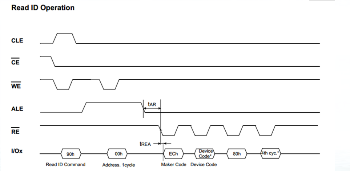
First, enable CE film selection
1) enabling CLE
2) Send 0X90 command and WE write pulse
3) Reset CLE and enable ALE
4) Send 0X00 address and WE write pulse
5) Set CLE and ALE as low level
6)while to determine if NRE is low
7) Read out the data of 8 I / OS and send out the rising edge pulse of RE
1.2 introduction to NAND flash controller
There is a nand flash controller in 2440, which can automatically control the control pins of CLE and ale. We just need to configure the controller, and then we can directly write the command, write the address, read and write the data to its register (before reading and writing the data, we need to judge the RnB pin), as shown in the following figure:
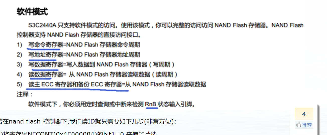
If we read ID under nand flash controller, we only need the following steps (very convenient):
1) Set bit1=0 of register nfcont (0x4e0000004) to enable chip selection
2) Write register NFCMMD(0x4E000008)=0X90, send command
3) Write register NFADDR(0x4E00000C)=0X00, send address
4)while to determine if NRE is low
5) Read the register NFDATA(0x4E000010) to read the data
1.3 we test in uboot to read ID through md and mw commands (x should be lowercase)
As shown in the figure below, read out 0xec 0xda 0x10 0x95 finally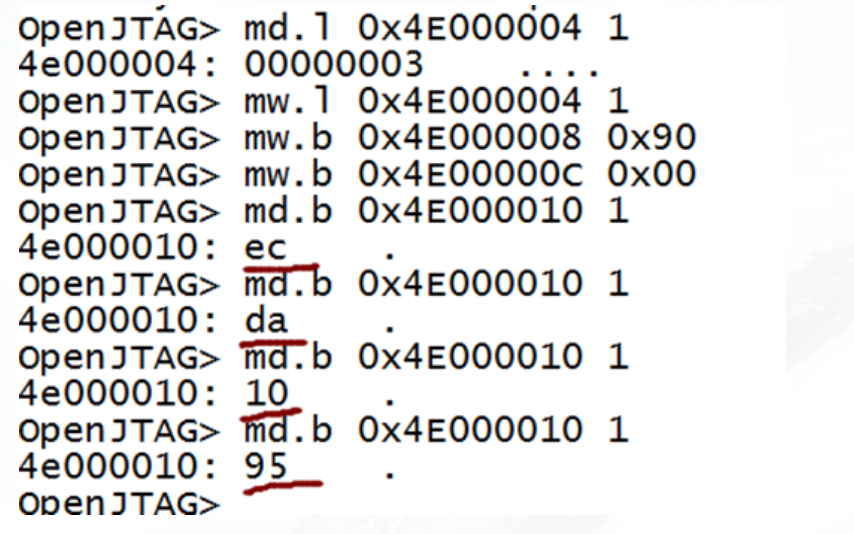
It just corresponds to the data in our nand flash manual (where 0XEC represents the manufacturer ID, 0X1).
2 next, we will refer to the nand flash driver, which is located in drivers/mtd/nand/s3c2410.c
2.1 why is nand in the mtd directory?
Because mtd(memory technology device storage technology device) is a subsystem of Linux used to access memory devices (ROM, flash). The main purpose of MTD is to make the driver of the new memory device simpler, so it provides an abstract interface between the hardware and the upper layer.
2.2 first, let's look at the entry function of s3c2410.c:
static int __init s3c2410_nand_init(void)
{
       printk("S3C24XX NAND Driver, (c) 2004 Simtec Electronics\n");
       platform_driver_register(&s3c2412_nand_driver);
       platform_driver_register(&s3c2440_nand_driver);

       return platform_driver_register(&s3c2410_nand_driver);
}
In the entry function, a platform device driver is registered, that is to say, when it matches the nandflash device, S3C2440 NAND driver - > probe will be called to initialize
Let's go into the probe function and see how it initializes
static int s3c24xx_nand_probe(struct platform_device *pdev, enum s3c_cpu_type cpu_type)
{
... ...

err = s3c2410_nand_inithw(info, pdev);       //Initialize hardware, set TACLS, TWRPH0, TWRPH1 communication timing, etc

s3c2410_nand_init_chip(info, nmtd, sets);    //Initialization chip

nmtd->scan_res = nand_scan(&nmtd->mtd, (sets) ? sets->nr_chips : 1); //3. Scan nandflash
... ...
s3c2410_nand_add_partition(info, nmtd, sets);         //4. Call add mtd partitions() to add mtd partitions
... ...
}
Through the above code and comments, it can be concluded that the driver mainly calls the NAND scan() function and add MTD partitions() function of the kernel to complete the registration of nandflash.
3. The scan function of NAND ˊ scan() in probe() above is located in / Drivers / MTD / NAND / NAND ˊ base. C
It will call NAND ﹣ scan() - > NAND ﹣ scan ﹣ ident() - > NAND ﹣ get ﹣ flash ﹣ type() to get the type of flash memory
And NAND scan() - > NAND scan ident() - > NAND scan tail() to construct members of mtd devices (to read, write, erase nandflash, etc.)
3.1 the nand_get_flash_type() function is as follows:
static struct nand_flash_dev *nand_get_flash_type(struct mtd_info *mtd,struct nand_chip *chip,int busw, int *maf_id)
{
 struct nand_flash_dev *type = NULL;
 int i, dev_id, maf_idx;
 chip->select_chip(mtd, 0);     //Call the member of NAND ABCD structure select ABCD enable flash selection

 chip->cmdfunc(mtd, NAND_CMD_READID, 0x00, -1); //3.2 call cmdfunc, a member of NAND ABCD structure, send read id command, and save the data in mtd structure

 *maf_id = chip->read_byte(mtd); // Get the manufacturer ID,

  dev_id = chip->read_byte(mtd);   //Get device ID

   /* 3.3for Loop match NAND flash IDS [] array to find the corresponding NAND flash information*/
     for (i = 0; nand_flash_ids[i].name != NULL; i++)
   {
         if (dev_id == nand_flash_ids[i].id)     //Match device ID
         {type =  &nand_flash_ids[i];
           break;}
  }
       ... ...

/* 3.4 If the match is successful, the nandflash parameter will be printed   */
printk(KERN_INFO "NAND device: Manufacturer ID:"
                     " 0x%02x, Chip ID: 0x%02x (%s %s)\n", *maf_id,
                     dev_id, nand_manuf_ids[maf_idx].name, mtd->name);
       ... ...
}
From the above code and comments, it can be concluded that the NAND ABCD structure is to save the hardware related functions (this structure will be discussed later).
3.2 where NAND ﹣ CMD ﹣ readid is defined as 0X90, that is to say, send 0X90 command and 0x00 address to read id, and finally put it into mtd.
3.3 the nand flash IDS [] array is a global variable. Here, by matching the device ID, we can determine how big our nand flash is
As shown in the following figure, in the chip manual, you can see that the device ID of nand flash = 0xda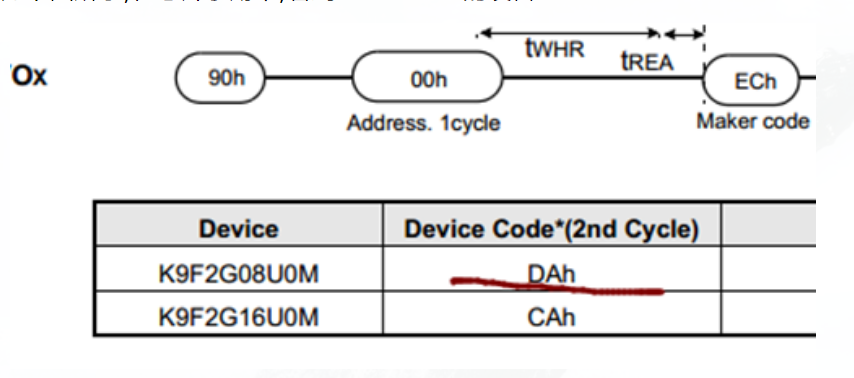
So it matches the 0XDA in NAND flash IDS []:
3.4 then print out the nand flash parameter. When we start the kernel, we can see:

4.1 the prototype of the add MTD partitions() function is as follows:
int add_mtd_partitions(struct mtd_info *master, const struct mtd_partition *parts,int nbparts);  //Create multiple partition mtd devices
//Introduction to the letter:
//master: the mtd device to be created
//parts: an array of partition information. Its structure is MTD [partition], which is as follows:
/*
struct mtd_partition {
       char *name;                  //Partition name, such as bootloader, params, kernel, root
       u_int32_t size;               //Partition size
       u_int32_t offset;            //Offset value of the partition
       u_int32_t mask_flags;            //Mask mark
       struct nand_ecclayout *ecclayout; //OOB layout
       struct mtd_info **mtdp;              //MTD Pointer to, not commonly used
};
*/
//nbparts: equal to the number of arrays of partition information, indicating the number of partitions to be created
For example, when we start the kernel, we can also find the partition information of nandflash that comes with the kernel: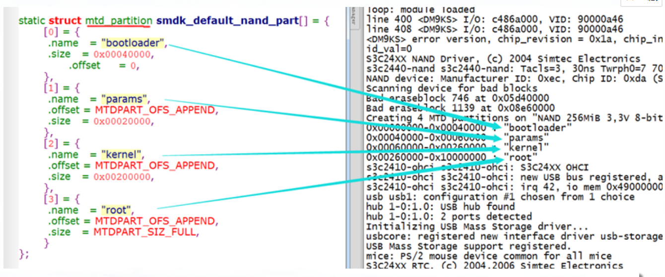
4.2 where the add ﹣ MTD ﹣ device() function is as follows:
int add_mtd_device(struct mtd_info *mtd)    //Create an mtd device
{
 struct list_head *this;
 ... ...
    list_for_each(this, &mtd_notifiers)     //4.3 find the list head structure in the MTD [notifiers] list
  {
   struct mtd_notifier *not = list_entry(this, struct mtd_notifier, list); //Find struct MTD? Notifier * not through list? Head
   not->add(mtd);            //Finally, call the add() function of mtd_notifier.
  }
 ... ...
}
4.3 we search the MTD "notifiers" list in the above function
Look at the list head structure inside, where it is put in, and you can find out what the add() is.
4.4 as shown in the figure below, it is found that the list head is placed in the MTD notifiers list in register MTD user()
4.5 continue to search register? MTD? User(), by which call

As shown in the figure above, it is called by drivers/mtd/mtdchar.c, drivers/mtd/mtd_blkdevs.c (sections 4.6 and 4.7 will be analyzed)
The reason is that the MTD layer not only provides the operation interface of character device (mtdchar.c), but also implements the operation interface of block device (mtd_blkdevs.c)
We can also find the block MTD device node and character MTD device node by entering ls -l /dev/mtd * in the console, as shown in the following figure: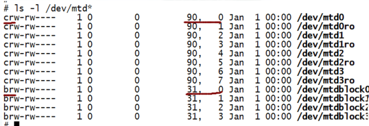
In the above figure, you can see that there are four partitions of devices, each of which contains two character devices (mtd%d,mtd%dro) and a block device (mtdblock0)
The main device number of MTD's block device is 31, and the main device number of MTD's character device is 90 (where will be created later).
4.6 enter drivers/mtd/mtdchar.c found above, and its entry function is init? Mtdchar():
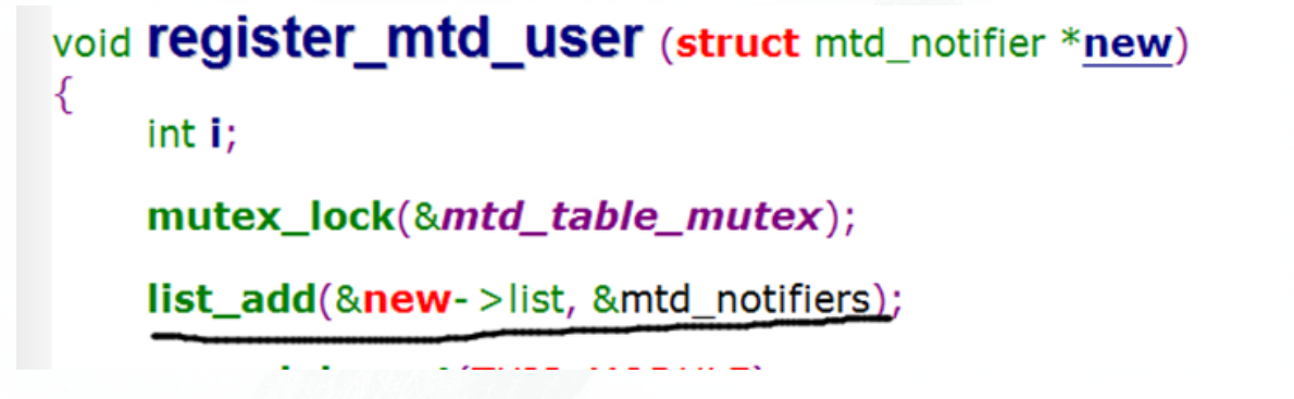
static int __init init_mtdchar(void) { /*Create a character device mtd with the main device number of 90, which can be seen by cat / proc / devices */ if (register_chrdev(MTD_CHAR_MAJOR, "mtd", &mtd_fops)) { printk(KERN_NOTICE "Can't allocate major number %d for Memory Technology Devices.\n",MTD_CHAR_MAJOR); return -EAGAIN; } mtd_class = class_create(THIS_MODULE, "mtd"); //Create class if (IS_ERR(mtd_class)) { printk(KERN_ERR "Error creating mtd class.\n"); unregister_chrdev(MTD_CHAR_MAJOR, "mtd"); return PTR_ERR(mtd_class); } register_mtd_user(¬ifier); //Call register? MTD? User() to add the notifier to the MTD? Notifiers list return 0; }
The reason why the device node is not created above is that there is no nand flash driver at this time.
4.6.1 it is found that the above notifiers are of MTD ﹣ notifier structure:
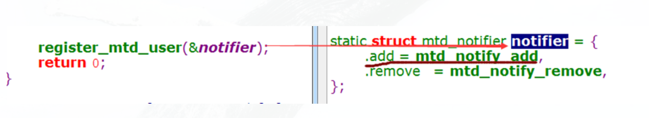
4.6.2 as shown in the figure above, enter the MTD notify add() function of notify to see:
static void mtd_notify_add(struct mtd_info* mtd)
{
       if (!mtd)
              return;

       /*Where MTD char major main equipment is defined as 90 */
       class_device_create(mtd_class, NULL, MKDEV(MTD_CHAR_MAJOR, mtd->index*2),NULL, "mtd%d", mtd->index);
                                                        //Create mtd%d character device node

       class_device_create(mtd_class, NULL,MKDEV(MTD_CHAR_MAJOR, mtd->index*2+1),NULL, "mtd%dro", mtd->index);
                                   //Create mtd%dro character device node

}
This function creates two character devices (MTD% D, MTD% d ro), where the character device of ro is read-only
Summed up:
The entry function of mtdchar.c adds the notice to the MTD "notifie rs" list,
Then when the list head of the mtd character device is found in the add? mtd? Device() function, mtd? Notifiers - > add() is called to create a two character device (mtd%d,mtd%dro).
4.7 in the same way, we also enter MTD ﹣ blkdevs. C (MTD block device), and find the blktrans ﹣ notifier variable registered in the MTD ﹣ notifiers list:
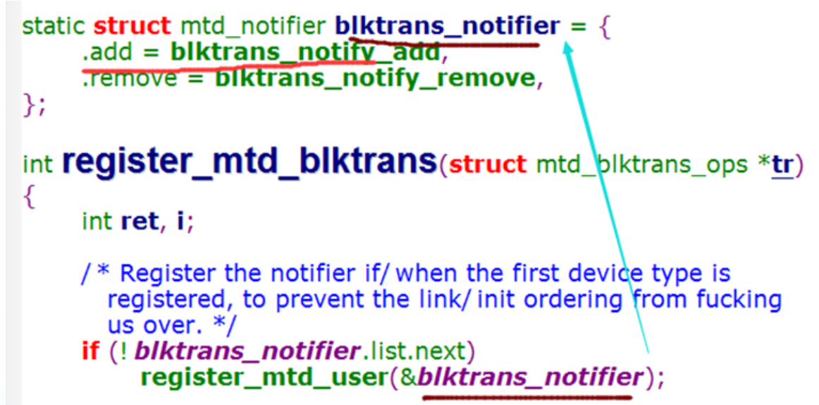
4.7.1 then enter the blktrans [notify] add() function of the blktrans [notifier variable:
static void blktrans_notify_add(struct mtd_info *mtd)
{
       struct list_head *this;

       if (mtd->type == MTD_ABSENT)
              return;

       list_for_each(this, &blktrans_majors) //Find the list head structure in the blktrans ﹣ major list
    {
        struct mtd_blktrans_ops *tr = list_entry(this, struct mtd_blktrans_ops, list);
        tr->add_mtd(tr, mtd);    // Execute add mtd() of the MTD blktrans OPS structure
       }
}
From the above code and comments, it can be concluded that the add() of the block device is to look up the blktrans ﹣ major list, and then execute the add ﹣ mtd() of the MTD ﹣ blktrans ﹣ OPS structure.
4.7.2 we search the link list of blktrans ﹣ major to see where the MTD ﹣ blktrans ﹣ OPS structure is added
Find the list in the register? MTD? Blktrans() function:
int register_mtd_blktrans(struct mtd_blktrans_ops *tr)
{
       ... ...
ret = register_blkdev(tr->major, tr->name);              //Register block device
tr->blkcore_priv->rq=blk_init_queue(mtd_blktrans_request, &tr->blkcore_priv->queue_lock);
                                                                             //Assign a request queue
... ...
       list_add(&tr->list, &blktrans_majors);                //Add tr - > list to the blktrans ﹣ major list
}
Continue to search register? MTD? Blktrans(), as shown in the figure below, and find that it is called by drivers/mtd/Mtdblock.c and mtdblock? Ro. C.
4.7.3 enter the drivers/mtd/Mtdblock.c function, as shown in the following figure:
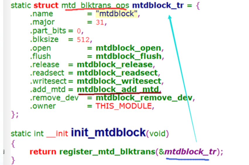
Find the add mtd() function to execute the MTD blktrans OPS structure, which is the mtdblock add mtd() function in the figure above
Add? MTD? Blktrans? Dev() is finally called in the mtdblock? Add? Mtd() function
4.7.4 the add? MTD? Blktrans? Dev() function is as follows
int add_mtd_blktrans_dev(struct mtd_blktrans_dev *new)
{
       ... ...
       gd = alloc_disk(1 << tr->part_bits);                  //Assign a gendisk structure

       gd->major = tr->major;                                //Set the primary device number of gendisk

       gd->first_minor = (new->devnum) << tr->part_bits;      //Set the start of gendisk this device number

       gd->fops = &mtd_blktrans_ops;                         //Set operation function
       ... ...

       gd->queue = tr->blkcore_priv->rq;           //Set request queue

       add_disk(gd);                                           //Register the gendisk structure with the kernel
}
Summed up:
The entry function of MTD ﹣ blkdevs() block device adds blktrans ﹣ notifier to the MTD ﹣ notifiers list, and creates a block device and a request queue
Then in the add ﹐ MTD ﹐ device() function, when blktrans ﹐ notifier is found, blktrans ﹐ notifier - > add() is called to allocate the registered gendisk structure.
5. Obviously in the kernel, mtd has helped us build the whole framework, and our nand flash driver only needs the following steps:
1) Set MTD? Info structure member
2) Set up NAND ABCD structure members
3) Set hardware correlation (set nand controller timing, etc.)
4) Scan nandflash through nand_scan()
5) Add partition by adding MTD partition() to create MTD character / block device
5.1 introduction to mtd_info structure:
It mainly implements the read(), write(), read ﹣ oob(), write ﹣ oob(), erase() and other operations of nandflash, which belongs to the software part. It will find the corresponding NAND ﹣ chip structure through its member priv to call the hardware related operations
5.2 introduction to NAND ABCD structure:
It is a priv member of MTD ﹣ info structure. It mainly describes NAND flash hardware in MTD device
When we do not set the members of nand_chip, the following members will be automatically set as default values by mtd. The code is located in: nand_scan() - > nand_scan_ident() - > nand_set_defaults ()
struct nand_chip {
    void  __iomem      *IO_ADDR_R;         /* nandflash address to read data */
    void  __iomem      *IO_ADDR_W;        /* nandflash address to write data to */

       /* Read a byte from the chip */
       uint8_t    (*read_byte)(struct mtd_info *mtd);
       /* Read a word from the chip */
       u16         (*read_word)(struct mtd_info *mtd);
       /* Write buffer contents to nandflash address, len: data length*/
       void (*write_buf)(struct mtd_info *mtd, const uint8_t *buf, int len);
       /* Read nandflash address to buffer, len: data length   */
       void (*read_buf)(struct mtd_info *mtd, uint8_t *buf, int len);
       /* Verify the data in the chip and write buffer */
       int          (*verify_buf)(struct mtd_info *mtd, const uint8_t *buf, int len);
    /* Select the chip. When chip==0, it means selected. When chip==-1, it means unchecked */
    void (*select_chip)(struct mtd_info *mtd, int chip);
       /* Check whether there is a bad block */
       int          (*block_bad)(struct mtd_info *mtd, loff_t ofs, int getchip);

       /* Mark bad block */
       int          (*block_markbad)(struct mtd_info *mtd, loff_t ofs);

    /* Command, address control function, dat: command / address to be transmitted */
    /*When bit[1]==1: indicates that the dat to be sent is a command
                bit[2]==1: Indicates that the dat to be sent is the address
                bit[0]==1: Indicates enable nand, = = 0: indicates disable nand
        Refer to the NAND command LP () function of the kernel for details. It will call the CMD crtl function to realize the function*/
      void (*cmd_ctrl)(struct mtd_info *mtd, int dat,unsigned int ctrl);

    /* Whether the device is ready. When the data of RnB pin returned by this function is equal to 1, it means that nandflash is ready */
    int (*dev_ready)(struct mtd_info *mtd);
    /* Realize command sending, and finally call NAND ABCD CMD ABCD Ctrl to realize  */
       void (*cmdfunc)(struct mtd_info *mtd, unsigned command, int column, int page_addr);
       /*Wait function, wait for nandflash to be ready through nand_chip - > dev_ready */
       int          (*waitfunc)(struct mtd_info *mtd, struct nand_chip *this);
       /* Processing of erase command */
       void (*erase_cmd)(struct mtd_info *mtd, int page);
       /* Scan bad block */
       int          (*scan_bbt)(struct mtd_info *mtd);
       int          (*errstat)(struct mtd_info *mtd, struct nand_chip *this, int state, int status, int page);
       /* Write a page */
       int          (*write_page)(struct mtd_info *mtd, struct nand_chip *chip,const uint8_t *buf, int page, int cached, int raw);

       int          chip_delay;                   /* Delay time determined by board */

       /* Some options related to specific nand chips are 8-bit wide nand by default,
     For example, setting nand? Bus width? 16 means that nand's bus width is 16 */
       unsigned int   options;


       /* page size of NAND chip represented by bit, such as a NAND chip
        * A page of has 512 bytes, so page "shift" is 9
        */
       int          page_shift;

       /* The erasable size of NAND chip in bits, such as the erasable size of a NAND chip
        * Erase 16K bytes (usually the size of a block), then the physical "erase" shift is 14
        */
       int          phys_erase_shift;

       /* The size of the bad block table expressed in bits, usually a bbt occupies a block,
        * So BBT \ erase \ shift is usually equal to physics \ erase \ shift
        */
       int          bbt_erase_shift;
       /* The capacity of NAND chip expressed in bits */
       int          chip_shift;
       /* NADN FLASH Number of chips */
       int          numchips;
       /* NAND Chip size */
       uint64_t chipsize;

       int          pagemask;
       int          pagebuf;
       int          subpagesize;
       uint8_t    cellinfo;
       int          badblockpos;
       nand_state_t   state;
       uint8_t           *oob_poi;
       struct nand_hw_control  *controller;
       struct nand_ecclayout   *ecclayout;     /* ECC layout */
/* ECC Check the structure. If it is not set, ecc.mode defaults to NAND ﹣ ECC ﹣ none */
/*It can be used for hardware ECC and software ECC verification, such as setting ECC. Mode = NAND? ECC? Soft (software ECC verification)*/
    struct nand_ecc_ctrl ecc;
       struct nand_buffers *buffers;
       struct nand_hw_control hwcontrol;
       struct mtd_oob_ops ops;
       uint8_t           *bbt;
       struct nand_bbt_descr   *bbt_td;
       struct nand_bbt_descr   *bbt_md;
       struct nand_bbt_descr   *badblock_pattern;
       void        *priv;
};
5.3 in this section, we need to set the members of NAND ABCD as follows:
IO? Addr? R (provide read data)
IO? Addr? W (write data provided)
Select [chip]
CMD? Ctrl (provide write command / address)
Dev_ready (provide RnB pin of nandflash to judge whether it is ready)
Ecc.mode (set ECC as hardware verification / software verification)
Other members will be set to the default value through NAND < scan() - > NAND < identity() - > NAND < set < defaults()
6. Next, we will write nand flash device driver
Reference: Drivers / MTD / NAND / at91 NAND. C
drivers/mtd/nand/s3c2410.c
6.1 the functions to be used in this section are as follows:
int nand_scan(struct mtd_info *mtd, int maxchips);   //Scan nandflash, return 0 after scanning successfully

int add_mtd_partitions(struct mtd_info *master,const struct mtd_partition *parts,int nbparts);
//Divide nandflash into nbparts partitions, multiple MTD character / block devices will be created, and 0 will be returned successfully
//master: the mtd device to be created
//parts: an array of partition information. Its structure is MTD [partition]
//nbparts: the number of partitions to create, such as the figure above, is equal to 4

int del_mtd_partitions(struct mtd_info *master);
//Unmount partition and unmount MTD character / block device
6.2 in the init entry function
1) Allocate the structure through kzalloc(): mtd_info and nand_chip
2) Obtain the virtual address of nand flash register through ioremap()
3) Set MTD? Info structure member
4) Set up NAND ABCD structure members
5) Set up hardware related
->5.1) enable nand flash clock through clk_get() and clk_enable()
->5.2) set timing
->5.3) turn off the selection and turn on the nand flash controller
6) Scan nandflash through nand_scan()
7) Add partition by adding MTD partition() to create MTD character / block device
6.3 in the exit entry function
1) Unload partition, unload character / block device
2) release mtd
3) Release nand flash register
4) Release NAND ABCD chip
The driver code is as follows:
#include <linux/module.h>
#include <linux/types.h>
#include <linux/init.h>
#include <linux/kernel.h>
#include <linux/string.h>
#include <linux/ioport.h>
#include <linux/platform_device.h>
#include <linux/delay.h>
#include <linux/err.h>
#include <linux/slab.h>
#include <linux/clk.h>
#include <linux/mtd/mtd.h>
#include <linux/mtd/nand.h>
#include <linux/mtd/nand_ecc.h>
#include <linux/mtd/partitions.h>
#include <asm/io.h>
#include <asm/arch/regs-nand.h>
#include <asm/arch/nand.h>

struct  mynand_regs {
    unsigned long nfconf  ;             //0x4E000000
    unsigned long nfcont  ;
    unsigned long nfcmd   ;
    unsigned long nfaddr  ;
    unsigned long nfdata  ;
    unsigned long nfeccd0 ;
    unsigned long nfeccd1 ;
    unsigned long nfeccd  ;
    unsigned long nfstat  ;
    unsigned long nfestat0;
    unsigned long nfestat1;
    unsigned long nfmecc0 ;
    unsigned long nfmecc1 ;
    unsigned long nfsecc  ;
    unsigned long nfsblk  ;
    unsigned long nfeblk  ;
};
static struct mynand_regs *my_regs;              //nand register
static struct mtd_info *my_mtd;
static struct nand_chip *mynand_chip;

static struct mtd_partition mynand_part[] = {
    [0] = {
        .name   = "bootloader",
        .size   = 0x00040000,
        .offset    = 0,
    },
    [1] = {
        .name   = "params",
        .offset = MTDPART_OFS_APPEND,
        .size   = 0x00020000,
    },
    [2] = {
        .name   = "kernel",
        .offset = MTDPART_OFS_APPEND,
        .size   = 0x00200000,
    },
    [3] = {
        .name   = "root",
        .offset = MTDPART_OFS_APPEND,
        .size   = MTDPART_SIZ_FULL,
    }
};

  /*nand flash  :CE */
static void mynand_select_chip(struct mtd_info *mtd, int chipnr)
{
        if(chipnr==-1)          //CE Disable
       {
        my_regs->nfcont|=(0x01<<1);               //bit1 set 1
       }
        else                         //CE Enable
       {
        my_regs->nfcont&=~(0x01<<1);        //bit1 set 0
       }
}
   /*Command / address control function */
static void mynand__cmd_ctrl(struct mtd_info *mtd, int dat, unsigned int ctrl)
{
    if (ctrl & NAND_CLE)                       //The current status is command,
          my_regs->nfcmd=dat;
    else                   //Current address status, if (ctrl & nand_ale)
         my_regs->nfaddr=dat;
}

/* nand flash Device ready function (get RnB pin status */
static int mynand__device_ready(struct mtd_info *mtd)
{
    return (my_regs->nfstat&0x01);                //Get RnB status, 0: busy 1: ready
}


    /*init Entrance function*/
static int mynand_init(void)
{
    struct clk *nand_clk;
    int res;
   /*1.Allocation structure: MTD ﹣ info and NAND ﹣ chip */
   my_mtd=kzalloc(sizeof(struct mtd_info), GFP_KERNEL);
   mynand_chip=kzalloc(sizeof(struct nand_chip), GFP_KERNEL);

    /*2.Get the virtual address of nand flash register*/
     my_regs=ioremap(0x4E000000, sizeof(struct mynand_regs));

    /*3.Set MTD? Info*/
    my_mtd->owner=THIS_MODULE;
    my_mtd->priv=mynand_chip;                    //Private data

    /*4.Set up NAND ABCD chip*/
    mynand_chip->IO_ADDR_R=&my_regs->nfdata;                 //Set read data
    mynand_chip->IO_ADDR_W=&my_regs->nfdata;                 //Set write data
    mynand_chip->select_chip=mynand_select_chip;             //Set CE
    mynand_chip->cmd_ctrl = mynand__cmd_ctrl;                //Set write command/address
    mynand_chip->dev_ready = mynand__device_ready;           //Set RnB
    mynand_chip->ecc.mode = NAND_ECC_SOFT;                   //Set up software ECC


    /*5.Set up hardware related*/
        /*5.1 Enable nand flash clock*/
        nand_clk=clk_get(NULL,"nand");
        clk_enable(nand_clk);

        /*5.2 Setup timing*/
        #define TACLS       0                    //0nS
        #define TWRPH0   1                       //15nS
        #define TWRPH1   0                       //5nS
        my_regs->nfconf = (TACLS<<12) | (TWRPH0<<8) | (TWRPH1<<4);

        /*5.3       bit1:Turn off selection, bit0: turn on nand flash controller*/
        my_regs->nfcont=(1<<1)|(1<<0);

    /*6.Scanning NAND*/
    if (nand_scan(my_mtd, 1)) {                   // 1: Indicates that only one nand flash device is scanned
        res = -ENXIO;
        goto out;
    }

    /*7.Add partition, create character / block device*/
    res = add_mtd_partitions(my_mtd, mynand_part, 4);
    if(res)
    return 0;

out:
    del_mtd_partitions(my_mtd);                      //Unload partition, unload character / block device
    kfree(my_mtd);                                      //Release mtd
    iounmap(my_regs);                                //Release nand flash register
    kfree(mynand_chip);                             //Release NAND ABCD chip
    return 0;

}

/*exit Export function*/
static void mynand_exit(void)
{
    del_mtd_partitions(my_mtd);     //Unload partition, unload character / block device
    kfree(my_mtd);                          //Release mtd
    iounmap(my_regs);                    //Release nand flash register
    kfree(mynand_chip);                 //Release NAND ABCD chip
}

module_init(mynand_init);
module_exit(mynand_exit);
MODULE_LICENSE("GPL");

