This paper is a learning note based on Linux version number of mini2440 development board linux-2.6.32.2
I. probe function of I2S driver
- Mapping virtual memory, IIS register starting address is: 0x55000000
s3c24xx_i2s.regs = ioremap(S3C2410_PA_IIS, 0x100);
- Get iis clock and enable iis clock
s3c24xx_i2s.iis_clk = clk_get(&pdev->dev, "iis");
clk_enable(s3c24xx_i2s.iis_clk);
- Configuration IIS pins, IIS has five pins, respectively:
I2SLRCK: Represents the channel of the current voice transmission, I2SLRCK is low-level data transmission of the "left channel" and I2SLRCK is high-level data transmission of the "right channel".
I2SSCLK: Serial Bit Clock, I2S Transmission Data Use
SCDCLK:2440 provides the system clock for decoding chips.
I2SSDI: I2S input signal line
I2SSDO:I2S Output Signal Line
#define S3C2410_GPE0_I2SLRCK   (0x02 << 0)
#define S3C2410_GPE1_I2SSCLK   (0x02 << 2)
#define S3C2410_GPE2_CDCLK     (0x02 << 4)
#define S3C2410_GPE3_I2SSDI    (0x02 << 6)
#define S3C2410_GPE4_I2SSDO    (0x02 << 8)
/* Configure the I2S pins in correct mode */
s3c2410_gpio_cfgpin(S3C2410_GPE0, S3C2410_GPE0_I2SLRCK);
s3c2410_gpio_cfgpin(S3C2410_GPE1, S3C2410_GPE1_I2SSCLK);
s3c2410_gpio_cfgpin(S3C2410_GPE2, S3C2410_GPE2_CDCLK);
s3c2410_gpio_cfgpin(S3C2410_GPE3, S3C2410_GPE3_I2SSDI);
s3c2410_gpio_cfgpin(S3C2410_GPE4, S3C2410_GPE4_I2SSDO);
GPECON register: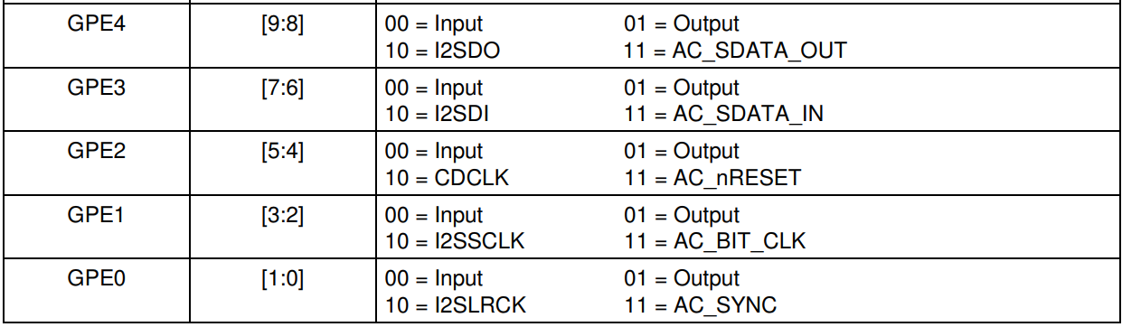
- I2S enable, bit 0 of IISCON register write 1
#define S3C2410_IISCON_IISEN	  (1<<0)
writel(S3C2410_IISCON_IISEN, s3c24xx_i2s.regs + S3C2410_IISCON);

- First control the sending and receiving stop of I2S, first do not send and receive.
s3c24xx_snd_txctrl(0);
s3c24xx_snd_rxctrl(0);
II. Transmission Control of I2S
- Start sending I2S
Write IISCON register, I2S enabled, DMA sent request enable, IISLRCK active
#define S3C2410_IISCON_TXDMAEN	  (1<<5)
#define S3C2410_IISCON_IISEN	  (1<<0)
#define S3C2410_IISCON_TXIDLE	  (1<<3)
iiscon  |= S3C2410_IISCON_TXDMAEN | S3C2410_IISCON_IISEN;
iiscon  &= ~S3C2410_IISCON_TXIDLE;


(2) Write IISFCON registers to send caches in DMA mode.
#define S3C2410_IISFCON_TXDMA	  (1<<15)
#define S3C2410_IISFCON_TXENABLE  (1<<13)
iisfcon |= S3C2410_IISFCON_TXDMA | S3C2410_IISFCON_TXENABLE;

(3) Write IISMOD register and select the sending mode of I2S.
#define S3C2410_IISMOD_TXMODE	  (2<<6)
iismod  |= S3C2410_IISMOD_TXMODE;

- Stop sending I2S
Stopping I2S is almost the opposite of the control of sending I2S. The only difference is that I2S is not disabled.
III. Receiving Control of I2S
- Start the reception of I2S
Write IISCON register, I2S enabled, DMA received request enable, IISLRCK active
#define S3C2410_IISCON_RXDMAEN	  (1<<4)
#define S3C2410_IISCON_IISEN	  (1<<0)
#define S3C2410_IISCON_RXIDLE	  (1<<2)
iiscon  |= S3C2410_IISCON_RXDMAEN | S3C2410_IISCON_IISEN;
iiscon  &= ~S3C2410_IISCON_RXIDLE;


(2) Write IISMOD register and select the receiving mode of I2S.
#define S3C2410_IISMOD_RXMODE	  (1<<6)
iismod  |= S3C2410_IISMOD_RXMODE;

(3) Write IISFCON registers to receive caches. The caching mode is DMA mode.
#define S3C2410_IISFCON_RXDMA	  (1<<14)
#define S3C2410_IISFCON_RXENABLE  (1<<12)
iisfcon |= S3C2410_IISFCON_RXDMA | S3C2410_IISFCON_RXENABLE;
- Stop receiving I2S
Write the opposite value to the boot register.
IV. Mode settings of I2S
- Master/slave mode settings, 8th bit settings of IISMOD registers
master mode: cpu provides clock to audio decoder chip
Slve mode: Audio decoder chip provides clock
iismod |= S3C2410_IISMOD_SLAVE;
writel(iismod, s3c24xx_i2s.regs + S3C2410_IISMOD);

- Setting Serial Data Format, Setting the 4th Bit of IISMOD Register
"#define S3C2410_IISMOD_MSB"	"  (1<<4)"
iismod |= S3C2410_IISMOD_MSB;

The chip only provides two data formats, one is MSB (LEFT) JUSTIFIED and the other is standard IIS format.
IIS format data is input the first data "MSB" (a SCLK clock over SD) after passing through a SCLK bit clock. Finally, it ends with "MSB".
The MSB format is that the first SCLK clock immediately outputs the first data.
V. s3c24xx_i2s_hw_params function of I2S
- Set s3c24xx_i2s_hw_params.dai.cpu_dai.dma_data, assuming it is playing now.
s3c24xx_i2s_hw_params.dai.cpu_dai.dma_data = s3c24xx_i2s_pcm_stereo_out
static struct s3c24xx_pcm_dma_params s3c24xx_i2s_pcm_stereo_out = {
	.client		= &s3c24xx_dma_client_out,
	.channel	= DMACH_I2S_OUT,
	.dma_addr	= S3C2410_PA_IIS + S3C2410_IISFIFO,
	.dma_size	= 2,
};
The address of IIS FIFO register is 0x55000010, and the size of register is 2 bytes.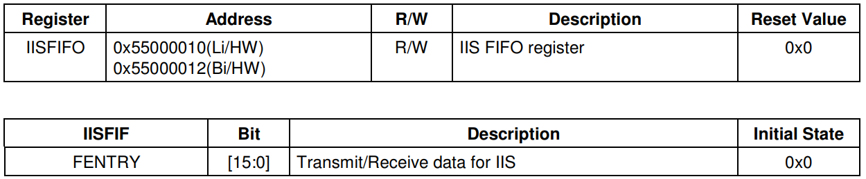
- Set the number of bits of data to be transmitted at a time
#define S3C2410_IISMOD_16BIT	  (1<<3)
iismod |= S3C2410_IISMOD_16BIT;
writel(iismod, s3c24xx_i2s.regs + S3C2410_IISMOD);

6. s3c24xx_i2s_trigger function
- Look at the playing state, judge the direction of substream, call s3c24xx_snd_txctrl(1) when playing, record and call s3c24xx_snd_rxctrl(1);
- Start DMA playback: s3c2410_dma_ctrl(channel, S3C2410_DMAOP_STARTED);
VII. IIS Clock Settings
- Clock source set to PCLK or MPLLin
#define S3C2440_IISMOD_MPLL	  (1<<9)
iismod |= S3C2440_IISMOD_MPLL;
writel(iismod, s3c24xx_i2s.regs + S3C2410_IISMOD);

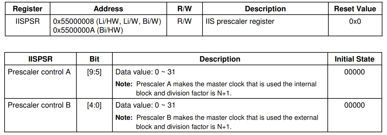
- Setting frequency dividing coefficient
writel(div, s3c24xx_i2s.regs + S3C2410_IISPSR);
reg = readl(s3c24xx_i2s.regs + S3C2410_IISCON);
writel(reg | S3C2410_IISCON_PSCEN, s3c24xx_i2s.regs + S3C2410_IISCON);

- Set master clock frequency, 256fs or 384fs
reg = readl(s3c24xx_i2s.regs + S3C2410_IISMOD) & ~(S3C2410_IISMOD_384FS);
writel(reg | div, s3c24xx_i2s.regs + S3C2410_IISMOD);

In summary, the sampling rate=(PCLK or MPLLin)/f frequency division coefficient/(256 or 384)
- Setting serial clock frequency
reg = readl(s3c24xx_i2s.regs + S3C2410_IISMOD) & ~S3C2410_IISMOD_FS_MASK;
writel(reg | div, s3c24xx_i2s.regs + S3C2410_IISMOD);

VIII. I2S Interface Registration
- Registration time: The s3c24xx_i2s_init function is called in the boot kernel. Register the I2S interface in the s3c24xx_i2s_init function.
module_init(s3c24xx_i2s_init);

static int __init s3c24xx_i2s_init(void)
{
	return snd_soc_register_dai(&s3c24xx_i2s_dai);
}
- Where to register: Register into a global list of dai_list s, which contain a variety of Dai interfaces.
int snd_soc_register_dai(struct snd_soc_dai *dai)
{
	if (!dai->name)
		return -EINVAL;

	/* The device should become mandatory over time */
	if (!dai->dev)
		printk(KERN_WARNING "No device for DAI %s\n", dai->name);

	if (!dai->ops)
		dai->ops = &null_dai_ops;

	INIT_LIST_HEAD(&dai->list);

	mutex_lock(&client_mutex);
	list_add(&dai->list, &dai_list);
	snd_soc_instantiate_cards();
	mutex_unlock(&client_mutex);

	pr_debug("Registered DAI '%s'\n", dai->name);

	return 0;
}
Nine. Conclusion
- The s3c24xx_i2s_dai interface is registered when the kernel is up.
- The s3c24xx_i2s_dai interface includes the settings of the I2S bus's baud rate and data transmission mode for the chip, and a hardware parameter operation set s3c24xx_i2s_dai_ops.
Reference Blog:
https://blog.csdn.net/gqb_driver/article/details/8551551