7.3 implementation of hummingbird E200 processor

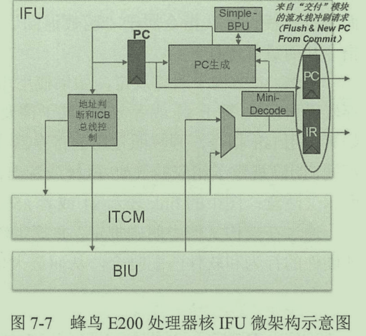
7.3.1 overall design idea of IFU
function
- Simply decode the retrieved address
- Simple branch prediction
- Generate fetched PC
- Access the ITCM or BIU according to the address of the PC

Address determination and ICB bus control module control access to ITCM and BIU. Hummingbird E200 is oriented to embedded scenarios with a small amount of code. Assuming that all codes are loaded and executed in ITCM, single cycle finger retrieval can be realized. If it needs to be read from external memory, it can be accessed through BIU. After the value is returned, it is decoded in the same clock cycle. If it is a branch jump instruction, simple BPU predicts in the same cycle. Finally, the decoding result and branch prediction result are used to generate the next instruction PC.
7.3.2 Mini-Decode
The mini decode module does not need to decode all the information, but only needs to obtain whether the instruction has branch jump, branch jump type and details.
Instantiate a complete decode and ignore some signals, so that the synthesis tool optimizes the irrelevant logic
`include "e203_defines.v"

module e203_ifu_minidec(

  //////////////////////////////////////////////////////////////
  // The IR stage to Decoder
  input  [`E203_INSTR_SIZE-1:0] instr,

  //////////////////////////////////////////////////////////////
  // The Decoded Info-Bus


  output dec_rs1en,
  output dec_rs2en,
  output [`E203_RFIDX_WIDTH-1:0] dec_rs1idx,
  output [`E203_RFIDX_WIDTH-1:0] dec_rs2idx,

  output dec_mulhsu,
  output dec_mul   ,
  output dec_div   ,
  output dec_rem   ,
  output dec_divu  ,
  output dec_remu  ,

  output dec_rv32,//Indicates that the current instruction is 16 bit or 32 bit
  output dec_bjp,//Indicates whether the current instruction is a branch jump instruction
  output dec_jal,//Is it a jal instruction
  output dec_jalr,//Is it a jalr instruction
  output dec_bxx,//Is it a conditional branch instruction
  output [`E203_RFIDX_WIDTH-1:0] dec_jalr_rs1idx,
  output [`E203_XLEN-1:0] dec_bjp_imm

  );

  e203_exu_decode u_e203_exu_decode(

  .i_instr(instr),
  .i_pc(`E203_PC_SIZE'b0),//Unused input signals are connected to 0
  .i_prdt_taken(1'b0),
  .i_muldiv_b2b(1'b0),

  .i_misalgn (1'b0),
  .i_buserr  (1'b0),

  .dbg_mode  (1'b0),

      .dec_misalgn(),//Unused output signals are suspended
  .dec_buserr(),
  .dec_ilegl(),

  .dec_rs1x0(),
  .dec_rs2x0(),
  .dec_rs1en(dec_rs1en),
  .dec_rs2en(dec_rs2en),
  .dec_rdwen(),
  .dec_rs1idx(dec_rs1idx),
  .dec_rs2idx(dec_rs2idx),
  .dec_rdidx(),
  .dec_info(),
  .dec_imm(),
  .dec_pc(),


  .dec_mulhsu(dec_mulhsu),
  .dec_mul   (dec_mul   ),
  .dec_div   (dec_div   ),
  .dec_rem   (dec_rem   ),
  .dec_divu  (dec_divu  ),
  .dec_remu  (dec_remu  ),

  .dec_rv32(dec_rv32),
  .dec_bjp (dec_bjp ),
  .dec_jal (dec_jal ),
  .dec_jalr(dec_jalr),
  .dec_bxx (dec_bxx ),

  .dec_jalr_rs1idx(dec_jalr_rs1idx),
  .dec_bjp_imm    (dec_bjp_imm    )
  );


endmodule
7.3.3 simple BPU branch prediction
`include "e203_defines.v"

module e203_ifu_litebpu(

  // Current PC
  input  [`E203_PC_SIZE-1:0] pc,

  // The mini-decoded info
  input  dec_jal,
  input  dec_jalr,
  input  dec_bxx,
  input  [`E203_XLEN-1:0] dec_bjp_imm,
  input  [`E203_RFIDX_WIDTH-1:0] dec_jalr_rs1idx,

  // The IR index and OITF status to be used for checking dependency
  input  oitf_empty,
  input  ir_empty,
  input  ir_rs1en,
  input  jalr_rs1idx_cam_irrdidx,

  // The add op to next-pc adder
  output bpu_wait,
  output prdt_taken,
  output [`E203_PC_SIZE-1:0] prdt_pc_add_op1,
  output [`E203_PC_SIZE-1:0] prdt_pc_add_op2,

  input  dec_i_valid,

  // The RS1 to read regfile
  output bpu2rf_rs1_ena,
  input  ir_valid_clr,
  input  [`E203_XLEN-1:0] rf2bpu_x1,
  input  [`E203_XLEN-1:0] rf2bpu_rs1,

  input  clk,
  input  rst_n
  );
  // The JAL and JALR is always jump, bxxx backward is predicted as taken
  assign prdt_taken   = (dec_jal | dec_jalr | (dec_bxx & dec_bjp_imm[`E203_XLEN-1]));  //dec_bjp_imm is the offset of the conditional jump instruction. If it is a negative number, it is a backward jump
  // The JALR with rs1 == x1 have dependency or xN have dependency
    wire dec_jalr_rs1x0 = (dec_jalr_rs1idx == `E203_RFIDX_WIDTH'd0);//Determine rs1 index number
  wire dec_jalr_rs1x1 = (dec_jalr_rs1idx == `E203_RFIDX_WIDTH'd1);
  wire dec_jalr_rs1xn = (~dec_jalr_rs1x0) & (~dec_jalr_rs1x1);

  wire jalr_rs1x1_dep = dec_i_valid & dec_jalr & dec_jalr_rs1x1 & ((~oitf_empty) | (jalr_rs1idx_cam_irrdidx));//Determine whether there is RAW data correlation
  wire jalr_rs1xn_dep = dec_i_valid & dec_jalr & dec_jalr_rs1xn & ((~oitf_empty) | (~ir_empty));

                      // If only depend to IR stage (OITF is empty), then if IR is under clearing, or
                          // it does not use RS1 index, then we can also treat it as non-dependency
  wire jalr_rs1xn_dep_ir_clr = (jalr_rs1xn_dep & oitf_empty & (~ir_empty)) & (ir_valid_clr | (~ir_rs1en));

  wire rs1xn_rdrf_r;
  wire rs1xn_rdrf_set = (~rs1xn_rdrf_r) & dec_i_valid & dec_jalr & dec_jalr_rs1xn & ((~jalr_rs1xn_dep) | jalr_rs1xn_dep_ir_clr);
  wire rs1xn_rdrf_clr = rs1xn_rdrf_r;
  wire rs1xn_rdrf_ena = rs1xn_rdrf_set |   rs1xn_rdrf_clr;
  wire rs1xn_rdrf_nxt = rs1xn_rdrf_set | (~rs1xn_rdrf_clr);

  sirv_gnrl_dfflr #(1) rs1xn_rdrf_dfflrs(rs1xn_rdrf_ena, rs1xn_rdrf_nxt, rs1xn_rdrf_r, clk, rst_n);

  assign bpu2rf_rs1_ena = rs1xn_rdrf_set;

  assign bpu_wait = jalr_rs1x1_dep | jalr_rs1xn_dep | rs1xn_rdrf_set;//If there is data correlation, wait

  assign prdt_pc_add_op1 = (dec_bxx | dec_jal) ? pc[`E203_PC_SIZE-1:0]
                         : (dec_jalr & dec_jalr_rs1x0) ? `E203_PC_SIZE'b0
                         : (dec_jalr & dec_jalr_rs1x1) ? rf2bpu_x1[`E203_PC_SIZE-1:0]
                         : rf2bpu_rs1[`E203_PC_SIZE-1:0];

    assign prdt_pc_add_op2 = dec_bjp_imm[`E203_PC_SIZE-1:0];  //Generate two operands and send them to the adder for calculation

endmodule
It can be seen that all the combinational logic in the code is completed by assign, and the triggers involved are instantiated by templates, which is conducive to the realization of the circuit desired by the author by the synthesis tool.
7.3.4 PC generation
PC Auto increment: if the current instruction is 32 bits, the next instruction is PC+4, otherwise + 2. Data input is calculated by a shared adder.
7.3.5 access to ITCM and BIU
Residual cache technology
- 64 bit SRAM reads out 64 bits each time, but IFU takes 32 bits each time. You can read directly without SRAM enable next time.
- If the address is not aligned, the current maximum 16 bits of SRAM can be stored in the remaining cache, and a new read operation can be initiated, and then the newly read low 16 bits and the data in the remaining cache can be spliced
- If the addresses are not aligned during non sequential finger fetching, using two cycles to read will result in a cycle performance waste, which is inevitable.
There are a lot of codes. I can't sort them out. Let's jump first
7.3.6 ITCM
64 bit ITCM can achieve lower power consumption overhead
- For SRAM with small capacity, 64 bits are more compact than 32 bits. Therefore, with the same capacity, the 64 bit data width area is smaller.
- Taking out 64 bits at a time can consume less dynamic power consumption