Note: qq:468001647
PWM is widely used in control, from single motor control to servo control to manipulator control. However, it would be very troublesome to call all the way PWM directly in the project. Engineers should pay more attention to the research of algorithm and debugging of products, rather than to the basic rated control of single-chip microcontroller. Moreover, if the official library provided by registers or ST is used directly, the project will become very messy, No. It is conducive to the later development. Here, I have established an engineering library, which can support 16-way PWM output of STM32F1 series.
The following is a detailed explanation of the project.
First, let's look at the output of a section of PWM. Take PWM1 as an example. Before that, I'll show you the distribution of PWM pins, as follows:
Let's take channel 1 of PWM1 as an example.
No more nonsense, code it:
			RCC->APB2ENR|=1<<11; 	//TIM1 Clock Enablation
			RCC->APB2ENR|=1<<2; //GPIOA Clock Enablation
			GPIOA->CRH&=0XFFFFFFF0;	//Settings before PA8 clearance
			GPIOA->CRH|=0X0000000B;	//Multiplexing function output

			TIM1->ARR=arr_init;			//Setting counter auto-reload value
			TIM1->PSC=psc_init;			//Predivider settings

			TIM1->CCMR1|=6<<4;  	//CH1 PWM1 mode
			TIM1->CCMR1|=1<<3; 		//CH1 preloading enablement
			TIM1->CCER|=1<<0;   	//OC1 Output Enablation
				TIM1->BDTR|=1<<15;   	//MOE Main Output Enablation

			TIM1->CR1=0x0080;   	//ARPE enable
			TIM1->CR1|=0x01;    	//Enabling timer 1

			TIM1->CCR1 =PWM_VAL;
This is a PWM initialization code. We analyze it block by block.
RCC - > APB2ENR |= 1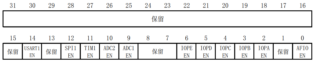
It is clear that to enable TIM1, the RCC_APB2ENR register must be located at 11 position 1, so that it can be enabled!
Okay, we activated TIM1 and then we have to enable it to output pins. This is PA8. So I won't introduce it much from the second line to the third line. It's worth noting that the pins here must be set as multiplexing function output.
TIM1 - > ARR = arr_init; // Set counter auto-reload value
TIM1 - > PSC = psc_init; / / Predivider settings
Comparing these two sentences is the most important part of PWM. It took me a lot of effort to understand this when I first learned it. Let me also briefly explain the principle here.
ARR refers to the automatic reload value and PSC refers to the pre-frequency value.
We know that F103 is basically the main frequency of 72MHZ, so the figure above is a period of waveform in a cycle. We divide a unit time into PSC segments, just like the sharp waves in the picture above (a sharp wave is a paragraph, a unit time has a PSC such a period). ARR is that each paragraph will reach a peak, the peak is ARR;
The two values are TIM1 - > ARR = arr_init; TIM1 - > PSC = psc_init;
Of course, here's a formula that needs special attention: frequency = 72000 000 000/((ARR+1) (PSC+1))*
Then we will talk about two modes of PWM: PWM1 and PWM2.
PWM1 mode: The CCRx on the graph is a value that you need to set (after that). In the same paragraph, it is high before counting CCRx, but once counting CCRx, it will become low. But when this paragraph ends, it will go to the next paragraph, and it will become high until the next one. The emergence of CCRx is repeated.
PWM2 mode: Contrary to PWM1 mode, in the same paragraph, the level before CCRx is low, and then high!
Then set the mode to a dedicated register: TIMx_CCMR1! 
We can see that,
Enabling PWM1, mode written as follows: TIM1 - > CCMR1 |= 6 < 4; // PWM1 mode
Enabling PWM2, mode as follows: TIM1 - > CCMR1 |= 7 < 4; //PWM2 mode
In this way, PWM mode enabled to complete, the following is pre-loading enablement, output enablement and total enablement, in particular: only TIM1 this advanced timer needs to enable MOE, TIM1 - > BDTR |= 1 < 15;!!
Here's the complete enabling process
TIM1 - > CCMR1 |= 1 < 3;//CH1 preloading enablement
TIM1 - > CCER |= 1 < 0; //OC1 output enablement
TIM1 - > BDTR |= 1 # 15; //MOE main output enablement
Here's the reference manual on the content I did not show one by one, interested can refer to, lazy words can be directly invoked!
However, it is worth mentioning that if the channel changes, the number of displacements must be changed. This reader can refer to the manual. I will give the code of other cases below.
The following is the power of ARPE, which can be directly invoked as above. Normally, the configuration will not change much.
		TIM1->CR1=0x0080;   	//ARPE enable
		TIM1->CR1|=0x01;    	//Enabling timer 1
Finally, the value of CCR1 is initialized (as follows, call directly, refer to above for explanation):
TIM1->CCR1 =PWM_VAL;
In this way, the PWM initialization statement is completed!!
Then if you need to change the duty cycle of PWM in main.c file, you can assign TIM1 - > CCR1 directly!!!
So, here's my programming habits:
1. I am used to PWM1
2. I normally assign PSC to 0 and ARR to 7199. Why?? This frequency F = 72,000,000/((7199+1)* (0+1)) = 10,000, i.e. 10,000 copies per minute, which is convenient and accurate!
The following is the PWM library I wrote:
#include "pwm.h"
/*
This library can support PWM pin channel control table:
Channel Name Corresponding Pin Multiplexed Pin
PWM1_CH1     PA8			PE9
PWM1_CH2	 PA9			PE11
PWM1_CH3	 PA10			PE13
PWM1_CH4	 PA11			PE14

PWM2_CH1     PA0            PA15
PWM2_CH2	 PA1			PB3
PWM2_CH3	 PA2			PB10
PWM2_CH4	 PA3			PB11

PWM3_CH1 	 PA6			PB4
PWM3_CH2	 PA7			PB5
PWM3_CH3	 PB0			PC8
PWM4_CH4	 PB1			PC9

PWM4_CH1	 PB6			PD12
PWM4_CH2	 PB7			PD13
PWM4_CH3	 PB8			PD14
PWM4_CH4	 PB9			PD15
*/

#define arr_init 7199// Frequency = 72000 000 000/((7199+1)*(0+1)), 10000 times per second
#define psc_init 0

/*
Function name: PWM initialization function
 Parameters: 1: PWM channel
	 II: Initial PWM value
 Time: 2019.8.14
 Example: PWM_Init(PWM1_CH1,0);
Note: This pwm initialization library can control the TIM1~TIM4 timing output of a total of 16 timers.
TIM1->CCMR1|=7<<4;  	//CH1 PWM2 The pattern applies to led
*/
void PWM_Init(PWM_Ch n,u16 PWM_VAL)
{
	switch(n)
	{
		case PWM1_CH1://PA8
		{
			RCC->APB2ENR|=1<<11; 	//TIM1 Clock Enablation
			RCC->APB2ENR|=1<<2; //GPIOA Clock Enablation
			GPIOA->CRH&=0XFFFFFFF0;	//Settings before PA8 clearance
			GPIOA->CRH|=0X0000000B;	//Multiplexing function output

			TIM1->ARR=arr_init;			//Setting counter auto-reload value
			TIM1->PSC=psc_init;			//Predivider settings

			TIM1->CCMR1|=6<<4;  	//CH1 PWM1 mode
			TIM1->CCMR1|=1<<3; 		//CH1 preloading enablement
			TIM1->CCER|=1<<0;   	//OC1 Output Enablation
				TIM1->BDTR|=1<<15;   	//MOE Main Output Enablation

			TIM1->CR1=0x0080;   	//ARPE enable
			TIM1->CR1|=0x01;    	//Enabling timer 1

			TIM1->CCR1 =PWM_VAL;

			break;
		}
		case PWM1_CH2://PA9
		{
			RCC->APB2ENR|=1<<11; 	//TIM1 Clock Enablation
			RCC->APB2ENR|=1<<2; //GPIOA Clock Enablation
			GPIOA->CRH&=0XFFFFFF0F;	//Settings before PA9 clears
			GPIOA->CRH|=0X000000B0;	//Multiplexing function output

			TIM1->ARR=arr_init;			//Setting counter auto-reload value
			TIM1->PSC=psc_init;			//Predivider settings

			TIM1->CCMR1|=6<<12;//CH2 PWM1 mode
			TIM1->CCMR1|=1<<11; //CH2 preloading enablement
			TIM1->CCER|=1<<4; //CH2 Output Enablation
				TIM1->BDTR |= 1<<15;//TIM1 must say this to output PWM

			TIM1->CR1=0x80; //ARPE enable
			TIM1->CR1|=0x01; //Enabling timer 2

			TIM1->CCR2 =PWM_VAL;

			break;
		}
		case PWM1_CH3://PA10
		{
			RCC->APB2ENR|=1<<11; 	//TIM1 Clock Enablation
			RCC->APB2ENR|=1<<2; //GPIOA Clock Enablation
			GPIOA->CRH&=0XFFFFF0FF;	//Settings before PA10 clears
			GPIOA->CRH|=0X00000B00;	//Multiplexing function output

			TIM1->ARR=arr_init;			//Setting counter auto-reload value
			TIM1->PSC=psc_init;			//Predivider settings

			TIM1->CCMR2|=6<<4;//CH2 PWM1 mode
			TIM1->CCMR2|=1<<3; //CH2 preloading enablement
			TIM1->CCER|=1<<8; //CH2 Output Enablation
				TIM1->BDTR |= 1<<15;//TIM1 must say this to output PWM

			TIM1->CR1=0x80; //ARPE enable
			TIM1->CR1|=0x01; //Enabling timer 2

			TIM1->CCR3 =PWM_VAL;

			break;
		}
		case PWM1_CH4://PA11
		{
			RCC->APB2ENR|=1<<11; 	//TIM1 Clock Enablation
			RCC->APB2ENR|=1<<2; //GPIOA Clock Enablation
			GPIOA->CRH&=0XFFFF0FFF;	//Settings before PA10 clears
			GPIOA->CRH|=0X0000B000;	//Multiplexing function output

			TIM1->ARR=arr_init;			//Setting counter auto-reload value
			TIM1->PSC=psc_init;			//Predivider settings

			TIM1->CCMR2|=6<<12;//CH2 PWM1 mode
			TIM1->CCMR2|=1<<11; //CH2 preloading enablement
			TIM1->CCER|=1<<12; //CH2 Output Enablation
				TIM1->BDTR |= 1<<15;//TIM1 must say this to output PWM

			TIM1->CR1=0x80; //ARPE enable
			TIM1->CR1|=0x01; //Enabling timer 2

			TIM1->CCR3 =PWM_VAL;

			break;
		}
		////////////////////////////////////////////////////////////////////////
		case PWM2_CH1://PA0
		{
			RCC->APB1ENR|=1; //Enabling TIM2 Clock
			RCC->APB2ENR|=1<<2; //GPIOA Clock Enablation
			GPIOA->CRL&=0XFFFFFFF0; //PA 0 reset
			GPIOA->CRL|=0X0000000B; //PA 0 Multiplexed Output

			TIM2->ARR=arr_init;//Setting counter auto-reload value
			TIM2->PSC=psc_init; //Predivider does not divide frequency

			TIM2->CCMR1|=6<<4; //CH1 PWM1 mode
			TIM2->CCMR1|=1<<3; //CH1 preloading enablement
			TIM2->CCER|=1<<0; //CH1 Output Enablation

			TIM2->CR1=0x80; //ARPE enable
			TIM2->CR1|=0x01; //Enabling timer 2

			TIM2->CCR1 =PWM_VAL;
		}
		case PWM2_CH2://PA1
		{
			RCC->APB1ENR|=1; //Enabling TIM2 Clock
			RCC->APB2ENR|=1<<2; //GPIOA Clock Enablation
			GPIOA->CRL&=0XFFFFFF0F; //PA 1 reset
			GPIOA->CRL|=0X000000B0; //PA 1 Multiplexed Output

			TIM2->ARR=arr_init;//Setting counter auto-reload value
			TIM2->PSC=psc_init; //Predivider does not divide frequency

			TIM2->CCMR1|=6<<12;//CH2 PWM1 mode
			TIM2->CCMR1|=1<<11; //CH2 preloading enablement
			TIM2->CCER|=1<<4; //CH2 Output Enablation

			TIM2->CR1=0x80; //ARPE enable
			TIM2->CR1|=0x01; //Enabling timer 2

			TIM2->CCR2 =PWM_VAL;
		}
		case PWM2_CH3://PA2
		{
			RCC->APB1ENR|=1; //Enabling TIM2 Clock
			RCC->APB2ENR|=1<<2; //GPIOA Clock Enablation
			GPIOA->CRL&=0XFFFFF0FF;	//Settings before PA2 clearance
			GPIOA->CRL|=0X00000B00;	//Multiplexing function output

			TIM2->ARR=arr_init;			//Setting counter auto-reload value
			TIM2->PSC=psc_init;			//Predivider settings

			TIM2->CCMR2|=6<<4;//CH3 PWM1 mode
			TIM2->CCMR2|=1<<3; //CH3 preloading enablement
			TIM2->CCER|=1<<8; //CH3 Output Enablation

			TIM2->CR1=0x80; //ARPE enable
			TIM2->CR1|=0x01; //Enabling timer 2

			TIM2->CCR3 =PWM_VAL;

			break;
		}
		case PWM2_CH4://PA3
		{
			RCC->APB1ENR|=1; //Enabling TIM2 Clock
			RCC->APB2ENR|=1<<2; //GPIOA Clock Enablation
			GPIOA->CRL&=0XFFFF0FFF;	//Settings before PA3 clearance
			GPIOA->CRL|=0X0000B000;	//Multiplexing function output

			TIM2->ARR=arr_init;			//Setting counter auto-reload value
			TIM2->PSC=psc_init;			//Predivider settings

			TIM2->CCMR2|=6<<12;//CH4 PWM1 mode
			TIM2->CCMR2|=1<<11; //CH4 preloading enablement
			TIM2->CCER|=1<<12; //CH4 Output Enablation

			TIM2->CR1=0x80; //ARPE enable
			TIM2->CR1|=0x01; //Enabling timer 2

			TIM2->CCR4 =PWM_VAL;

			break;
		}
		////////////////////////////////
		case PWM3_CH1://PA6
		{
			RCC->APB1ENR|=1<<1; //Enabling TIM3 Clock
			RCC->APB2ENR|=1<<2; //GPIOA Clock Enablation
			GPIOA->CRL&=0XF0FFFFFF; //PA6 reset
			GPIOA->CRL|=0X0B000000; //PA6 Multiplexed Output

			TIM3->ARR=arr_init;//Setting counter auto-reload value
			TIM3->PSC=psc_init; //Predivider does not divide frequency

			TIM3->CCMR1|=6<<4; //CH1 PWM1 mode
			TIM3->CCMR1|=1<<3; //CH1 preloading enablement
			TIM3->CCER|=1<<0; //CH1 Output Enablation

			TIM3->CR1=0x80; //ARPE enable
			TIM3->CR1|=0x01; //Enabling timer 2

			TIM3->CCR1 =PWM_VAL;

			break;
		}
		case PWM3_CH2://PA7
		{
			RCC->APB1ENR|=1<<1; //Enabling TIM3 Clock
			RCC->APB2ENR|=1<<2; //GPIOA Clock Enablation
			GPIOA->CRL&=0X0FFFFFFF; //PA7 reset
			GPIOA->CRL|=0XB0000000; //PA7 Multiplexed Output

			TIM3->ARR=arr_init;//Setting counter auto-reload value
			TIM3->PSC=psc_init; //Predivider does not divide frequency

			TIM3->CCMR1|=6<<12;//CH2 PWM1 mode
			TIM3->CCMR1|=1<<11; //CH2 preloading enablement
			TIM3->CCER|=1<<4; //CH2 Output Enablation

			TIM3->CR1=0x80; //ARPE enable
			TIM3->CR1|=0x01; //Enabling timer 2

			TIM3->CCR2 =PWM_VAL;

			break;
		}
		case PWM3_CH3://PB0
		{
			RCC->APB1ENR|=1<<1; //Enabling TIM3 Clock
			RCC->APB2ENR|=1<<3;
			GPIOB->CRL&=0XFFFFFFF0;	//Settings before PB0 clearance
			GPIOB->CRL|=0X0000000B;	//Multiplexing function output

			TIM3->ARR=arr_init;			//Setting counter auto-reload value
			TIM3->PSC=psc_init;			//Predivider settings

			TIM3->CCMR2|=6<<4;//CH3 PWM1 mode
			TIM3->CCMR2|=1<<3; //CH3 preloading enablement
			TIM3->CCER|=1<<8; //CH3 Output Enablation

			TIM3->CR1=0x80; //ARPE enable
			TIM3->CR1|=0x01; //Enabling timer 2

			TIM3->CCR3 =PWM_VAL;

			break;
		}
		case PWM3_CH4://PB1
		{
			RCC->APB1ENR|=1<<1; //Enabling TIM3 Clock
			RCC->APB2ENR|=1<<3;
			GPIOB->CRL&=0XFFFFFF0F;	//Settings before PB1 clearance
			GPIOB->CRL|=0X000000B0;	//Multiplexing function output

			TIM3->ARR=arr_init;			//Setting counter auto-reload value
			TIM3->PSC=psc_init;			//Predivider settings

			TIM3->CCMR2|=6<<12;//CH4 PWM1 mode
			TIM3->CCMR2|=1<<11; //CH4 preloading enablement
			TIM3->CCER|=1<<12; //CH4 Output Enablation

			TIM3->CR1=0x80; //ARPE enable
			TIM3->CR1|=0x01; //Enabling timer 2

			TIM3->CCR4 =PWM_VAL;

			break;
		}

		///////////////////////////////////
		case PWM4_CH1://PB6
		{
			RCC->APB1ENR|=1<<2; //Enabling TIM4 Clock
			RCC->APB2ENR|=1<<3; //GPIOB Clock Enablation
			GPIOB->CRL&=0XF0FFFFFF; //PB6 reset
			GPIOB->CRL|=0X0B000000; //PB6 Multiplexed Output

			TIM4->ARR=arr_init;//Setting counter auto-reload value
			TIM4->PSC=psc_init; //Predivider does not divide frequency

			TIM4->CCMR1|=6<<4; //CH1 PWM1 mode
			TIM4->CCMR1|=1<<3; //CH1 preloading enablement
			TIM4->CCER|=1<<0; //CH1 Output Enablation

			TIM4->CR1=0x80; //ARPE enable
			TIM4->CR1|=0x01; //Enabling timer 2

			TIM4->CCR1 =PWM_VAL;

			break;
		}
		case PWM4_CH2://PB7
		{
			RCC->APB1ENR|=1<<2; //Enabling TIM4 Clock
			RCC->APB2ENR|=1<<3; //GPIOB Clock Enablation
			GPIOB->CRL&=0X0FFFFFFF; //PB7 reset
			GPIOB->CRL|=0XB0000000; //PB7 multiplexing output

			TIM4->ARR=arr_init;//Setting counter auto-reload value
			TIM4->PSC=psc_init; //Predivider does not divide frequency

			TIM4->CCMR1|=6<<12;//CH2 PWM1 mode
			TIM4->CCMR1|=1<<11; //CH2 preloading enablement
			TIM4->CCER|=1<<4; //CH2 Output Enablation

			TIM4->CR1=0x80; //ARPE enable
			TIM4->CR1|=0x01; //Enabling timer 2

			TIM4->CCR2 =PWM_VAL;

			break;
		}
		case PWM4_CH3://PB8
		{
			RCC->APB1ENR|=1<<2; //Enabling TIM4 Clock
			RCC->APB2ENR|=1<<3; //GPIOB Clock Enablation
			GPIOB->CRH&=0XFFFFFFF0; //PB8 reset
			GPIOB->CRH|=0X0000000B; //PB8 multiplexed output

			TIM4->ARR=arr_init;//Setting counter auto-reload value
			TIM4->PSC=psc_init; //Predivider does not divide frequency

			TIM4->CCMR2|=6<<4;//CH3 PWM1 mode
			TIM4->CCMR2|=1<<3; //CH3 preloading enablement
			TIM4->CCER|=1<<8; //CH3 Output Enablation

			TIM4->CR1=0x80; //ARPE enable
			TIM4->CR1|=0x01; //Enabling timer 2

			TIM4->CCR3 =PWM_VAL;

			break;
		}
		case PWM4_CH4://PB9
		{
			RCC->APB1ENR|=1<<2; //Enabling TIM4 Clock
			RCC->APB2ENR|=1<<3; //GPIOB Clock Enablation
			GPIOB->CRH&=0XFFFFFF0F; //PB9 reset
			GPIOB->CRH|=0X000000B0; //PB9 multiplexed output

			TIM4->ARR=arr_init;//Setting counter auto-reload value
			TIM4->PSC=psc_init; //Predivider does not divide frequency

			TIM4->CCMR2|=6<<12;//CH4 PWM1 mode
			TIM4->CCMR2|=1<<11; //CH4 preloading enablement
			TIM4->CCER|=1<<12; //CH4 Output Enablation

			TIM4->CR1=0x80; //ARPE enable
			TIM4->CR1|=0x01; //Enabling timer 2

			TIM4->CCR4 =PWM_VAL;

			break;
		}
	}
}
/*
Function name: duty cycle setting function
 Parameters: 1: PWM channel
	 2: duty cycle (0-10000)
Time: 2019.8.14
 Example: PWM_duty(PWM1_CH1,1000);
*/
void PWM_duty(PWM_Ch n,u16 PWM_DUTY)
{
	float PWM_VAL;

	PWM_VAL=(arr_init*PWM_DUTY/10000.0);
	switch(n)
	{
		case PWM1_CH1://PA8
		{
			TIM1->CCR1 =PWM_VAL;
			break;
		}
		case PWM1_CH2://PA9
		{
			TIM1->CCR2 =PWM_VAL;
			break;
		}
		case PWM1_CH3://PA10
		{
			TIM1->CCR3 =PWM_VAL;
			break;
		}
		case PWM1_CH4://PA11
		{
			TIM1->CCR4 =PWM_VAL;
			break;
		}

		case PWM2_CH1://PA0
		{
			TIM2->CCR1 =PWM_VAL;
			break;
		}
		case PWM2_CH2://PA1
		{
			TIM2->CCR2 =PWM_VAL;
			break;
		}
		case PWM2_CH3://PA2
		{
			TIM2->CCR3 =PWM_VAL;
			break;
		}
		case PWM2_CH4://PA3
		{
			TIM2->CCR4 =PWM_VAL;
			break;
		}

		case PWM3_CH1://PA6
		{
			TIM3->CCR1 =PWM_VAL;
			break;
		}
		case PWM3_CH2://PA7
		{
			TIM3->CCR2 =PWM_VAL;
			break;
		}
		case PWM3_CH3://PB0
		{
			TIM3->CCR3 =PWM_VAL;
			break;
		}
		case PWM3_CH4://PB1
		{
			TIM3->CCR4 =PWM_VAL;
			break;
		}

		case PWM4_CH1://PB6
		{
			TIM4->CCR1 =PWM_VAL;
			break;
		}
		case PWM4_CH2://PB7
		{
			TIM4->CCR2 =PWM_VAL;
			break;
		}
		case PWM4_CH3://PB8
		{
			TIM4->CCR3 =PWM_VAL;
			break;
		}
		case PWM4_CH4://PB9
		{
			TIM4->CCR4 =PWM_VAL;
			break;
		}
	}
}
Here is the header file section
#ifndef __PWM_H
#define __PWM_H

#include "sys.h"

typedef enum
{
	PWM1_CH1,//TIM1_CH1,
	PWM1_CH2,//TIM1_CH2,
	PWM1_CH3,//TIM1_CH3,
	PWM1_CH4,//TIM1_CH4,

	PWM2_CH1,//TIM2_CH1,
	PWM2_CH2,//TIM2_CH2,
	PWM2_CH3,//TIM2_CH3,
	PWM2_CH4,//TIM2_CH4,

	PWM3_CH1,//TIM3_CH1,
	PWM3_CH2,//TIM3_CH2,
	PWM3_CH3,//TIM3_CH3,
	PWM3_CH4,//TIM3_CH4,

	PWM4_CH1,//TIM4_CH1,
	PWM4_CH2,//TIM4_CH2,
	PWM4_CH3,//TIM4_CH3,
	PWM4_CH4,//TIM4_CH4,

//	PWM5_CH1,//TIM5_CH1,
//	PWM5_CH2,//TIM5_CH2,
//	PWM5_CH3,//TIM5_CH3,
//	PWM5_CH4,//TIM5_CH4,
}PWM_Ch;

void PWM_Init(PWM_Ch n,u16 PWM_VAL);
void PWM_duty(PWM_Ch n,u16 PWM_DUTY);

#endif
If you use this library directly, you will find it really convenient. Let me give you an example.
void main ()
{
PWM_Init(PWM1_CH1,0); //Initialize PWM1 channel 1
while(1)
{
PWM_duty(PWM1_CH1,1000)// Set PWM to 1000, maximum 10000, or 10%;
}
}
So if you don't understand anything, or think there's something wrong with what I said above or in the library, you can always trust me and send me my personal qqq: 468001647.
I also very much hope that students who like single-chip technology can communicate with me and make progress together!!!
Note: qq:468001647