The main task of this paper is to realize the development of NAND FLASH driver with capacity 256MB and bit width 8 bits for JZ2440 development board board on board model K9F2G08U0A.
I. Pre-preparation
Development Board: JZ2440 (ARM9)
Kernel version: Linux-3.4.10
NAND FLASH : K9F2G08U0A( 256MB 8bit 3.3V)
Reconfigure the kernel and remove the existing NAND FLASH driver.
A Brief Introduction to K9F2G08U0A
NAND FLASH memory semiconductor designed by K9F2G08U0A Samsung Electronics is 256MB in size and 8bit in bit width, which supports ECC bad block detection mechanism.
1. schematic layout and basic pin definition
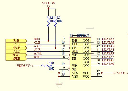
Specific definitions of pins:
LDATA0~LDATA7: Data, Address, Command Transfer Pin. What type of data to be transmitted is determined by ALE and CLE
RnB: A status judgment pin to determine whether flash is busy or ready
CLE: Command latch signal to send commands on high-level data lines
nFCE: Chip Selection Signal, Selected for Low Level Representation
ALE: Address latch pin to send addresses to high-level data lines
nFWE: Write signal, written on data line for low level
nFRE: Reading signals, representing reading data from data lines at low levels
2. Basic layout of storage unit
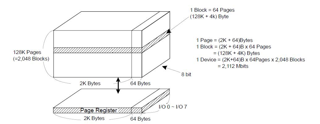
As can be seen from the figure above, the NAND flash stores data by pages, each of which is 2KB + 64Bytes in size. The first 2KB is used to store real data, and the latter 64Bytes data is used as ECC to check whether the page data is valid; each block contains 64 pages of data.
3. Implementation of Driver
1. Writing a driver for nand flash includes the following steps:
A. Assigning a nand_chip structural variable
b. Setting variables for this structure
c. Perform hardware-related operations
d. Use this structure variable and add device partitions
2. Realization
2.1 The basic work is as follows:
/* Define a structure to describe the register of s3c2440 nand controller */
struct yl_s3c_nand_regs {
	unsigned long nfconf  ;
	unsigned long nfcont  ;
	unsigned long nfcmd   ;
	unsigned long nfaddr  ;
	unsigned long nfdata  ;
	unsigned long nfeccd0 ;
	unsigned long nfeccd1 ;
	unsigned long nfeccd  ;
	unsigned long nfstat  ;
	unsigned long nfestat0;
	unsigned long nfestat1;
	unsigned long nfmecc0 ;
	unsigned long nfmecc1 ;
	unsigned long nfsecc  ;
	unsigned long nfsblk  ;
	unsigned long nfeblk  ;
};

/* Define a structure to facilitate nand-driven operations */
struct yl_nand_mtd{
	struct nand_chip *nand_chip;				// Define a pointer variable for a nand_chip structure
	struct mtd_info *mtd_info;					// Define a pointer variable for the mtd_info structure
	struct yl_s3c_nand_regs *s3c_nand_regs;		// Define a structure pointer variable for manipulating registers
	struct clk *clk;							// Define a structure pointer variable for operating clocks
};

/* Define a global variable of yl_nand_mtd structure */
static struct yl_nand_mtd nand_mtd;2.2. Hardware-related operations
/* 0,Hardware-related operations */
	/* 0.1 The address of the mapping register */
	nand_mtd.s3c_nand_regs = ioremap(0x4E000000, sizeof(struct yl_s3c_nand_regs));
	if (!nand_mtd.s3c_nand_regs) {
		printk("ioremap error!\n");
		ret = -ENOMEM;
		goto out1;
	}

	/* 0.2 Turn on the clock of nand controller */
	nand_mtd.clk = clk_get(NULL, "nand");
	if (IS_ERR(nand_mtd.clk)) {
		printk("clk_get error!\n");
		ret = -ENODEV;
		goto out2;
	}
	clk_enable(nand_mtd.clk);

	/* 0.3 Basic timing requirements for communication between nand controller and nand chip */
	/* Setting timing requirements */
#define tacls    0
#define twrph0   1
#define twrph1   0
	nand_mtd.s3c_nand_regs->nfconf = (tacls<<12) | (twrph0<<8) | (twrph1<<4);

	/* Setting up the state of nand controller: cancel chip selection to enable nand controller */
nand_mtd.s3c_nand_regs->nfcont = (1<<1) | (1<<0);2.3. Assign a nand_chip structure pointer variable
/* 1,Assignment of a nand_chip structural variable */
	nand_mtd.nand_chip = kzalloc(sizeof(struct nand_chip), GFP_KERNEL);
	if (!nand_mtd.nand_chip) {
		printk("kzalloc for nand_chip error!\n");
		ret = -ENOMEM;
		goto out3;
}This part mainly realizes three functions: yl_s3c_select_chip() setting chip selection, yl_s3c_cmd_ctrl() setting sending command or address, yl_s3c_dev_ready() judging whether nand flash is in ready state. Their specific implementation is as follows:/* 2,Set this structure variable */ nand_mtd.nand_chip->select_chip = yl_s3c_select_chip; // Setting function of chip selection signal nand_mtd.nand_chip->cmd_ctrl = yl_s3c_cmd_ctrl; // Control function to determine whether the data sent is a command or an address nand_mtd.nand_chip->dev_ready = yl_s3c_dev_ready; // Determine whether the chip is ready nand_mtd.nand_chip->IO_ADDR_R = &nand_mtd.s3c_nand_regs->nfdata; // Set the address of the register for reading data nand_mtd.nand_chip->IO_ADDR_W = &nand_mtd.s3c_nand_regs->nfdata; // Set the address of the register for writing data nand_mtd.nand_chip->ecc.mode = NAND_ECC_SOFT; // Setting ecc as software verification mode
Set the selection:
/* Setting the slice selection function of nand */
static void yl_s3c_select_chip(struct mtd_info *mtd, int chip)
{
if (-1 == chip) // Cancel slice selection, nfcont register bit[1] = 1
{
nand_mtd.s3c_nand_regs->nfcont |= (1<<1);
}
else // Check the nfcont register bit[1] = 0
{
nand_mtd.s3c_nand_regs->nfcont &= ~(1<<1);
}
}/* The command setup function determines whether the data sent is a command or an address */
static void yl_s3c_cmd_ctrl(struct mtd_info *mtd, int dat, unsigned int ctrl)
{
if (ctrl & NAND_CLE) // To issue orders
{
nand_mtd.s3c_nand_regs->nfcmd = dat;
}
else // Address
{
nand_mtd.s3c_nand_regs->nfaddr = dat;
}
}/* Judging the state of nand flash */
static int yl_s3c_dev_ready(struct mtd_info *mtd)
{
// nfstat register bit[0] = 0 busy, bit[0] = 1 ready
return (nand_mtd.s3c_nand_regs->nfstat & (1<<0));
}2.5 Using the nand_chip structure variable implemented above
/* 3,Use this structure variable */
/* Allocate mtd_info and link mtd_info to nand_chip */
nand_mtd.mtd_info = kzalloc(sizeof(struct mtd_info), GFP_KERNEL);
if (!nand_mtd.mtd_info) {
printk("kzalloc for mtd_info error!\n");
ret = -ENOMEM;
goto out4;
}
nand_mtd.mtd_info->owner = THIS_MODULE;
nand_mtd.mtd_info->priv = nand_mtd.nand_chip;
/* Recognize nand flash and construct mtd_info */
nand_scan(nand_mtd.mtd_info, 1);
/* 4,Adding partitions */ ret = mtd_device_parse_register(nand_mtd.mtd_info, NULL, NULL, yl_s3c_nand_partitions, ARRAY_SIZE(yl_s3c_nand_partitions));
To add partitions to this nand flash, we need to implement a partition table yl_s3c_nand_partitions, which is implemented as follows:
/* Define the partition table of nand flash */
static struct mtd_partition yl_s3c_nand_partitions[] =
{
[0] = {
.name = "bootloader",
.size = SZ_256K,
.offset = 0,
},
[1] = {
.name = "params",
.offset = MTDPART_OFS_APPEND,
.size = SZ_128K,
},
[2] = {
.name = "kernel",
.offset = MTDPART_OFS_APPEND,
.size = SZ_4M,
},
[3] = {
.name = "rootfs",
.offset = MTDPART_OFS_APPEND,
.size = MTDPART_SIZ_FULL,
}
};The complete implementation of the whole driver is as follows:
#include <linux/module.h>
#include <linux/types.h>
#include <linux/init.h>
#include <linux/kernel.h>
#include <linux/string.h>
#include <linux/ioport.h>
#include <linux/platform_device.h>
#include <linux/delay.h>
#include <linux/err.h>
#include <linux/slab.h>
#include <linux/clk.h>
#include <linux/cpufreq.h>
#include <linux/mtd/mtd.h>
#include <linux/mtd/nand.h>
#include <linux/mtd/nand_ecc.h>
#include <linux/mtd/partitions.h>
#include <asm/io.h>
#include <plat/regs-nand.h>
#include <plat/nand.h>
/* Define a structure to describe the register of s3c2440 nand controller */
struct yl_s3c_nand_regs {
unsigned long nfconf ;
unsigned long nfcont ;
unsigned long nfcmd ;
unsigned long nfaddr ;
unsigned long nfdata ;
unsigned long nfeccd0 ;
unsigned long nfeccd1 ;
unsigned long nfeccd ;
unsigned long nfstat ;
unsigned long nfestat0;
unsigned long nfestat1;
unsigned long nfmecc0 ;
unsigned long nfmecc1 ;
unsigned long nfsecc ;
unsigned long nfsblk ;
unsigned long nfeblk ;
};
/* Define a structure to facilitate nand-driven operations */
struct yl_nand_mtd{
struct nand_chip *nand_chip; // Define a pointer variable for a nand_chip structure
struct mtd_info *mtd_info; // Define a pointer variable for the mtd_info structure
struct yl_s3c_nand_regs *s3c_nand_regs; // Define a structure pointer variable for manipulating registers
struct clk *clk; // Define a structure pointer variable for operating clocks
};
/* Define a global variable of yl_nand_mtd structure */
static struct yl_nand_mtd nand_mtd;
/* Define the partition table of nand flash */
static struct mtd_partition yl_s3c_nand_partitions[] =
{
[0] = {
.name = "bootloader",
.size = SZ_256K,
.offset = 0,
},
[1] = {
.name = "params",
.offset = MTDPART_OFS_APPEND,
.size = SZ_128K,
},
[2] = {
.name = "kernel",
.offset = MTDPART_OFS_APPEND,
.size = SZ_4M,
},
[3] = {
.name = "rootfs",
.offset = MTDPART_OFS_APPEND,
.size = MTDPART_SIZ_FULL,
}
};
/* Setting the slice selection function of nand */
static void yl_s3c_select_chip(struct mtd_info *mtd, int chip)
{
if (-1 == chip) // Cancel slice selection, nfcont register bit[1] = 1
{
nand_mtd.s3c_nand_regs->nfcont |= (1<<1);
}
else // Check the nfcont register bit[1] = 0
{
nand_mtd.s3c_nand_regs->nfcont &= ~(1<<1);
}
}
/* The command setup function determines whether the data sent is a command or an address */
static void yl_s3c_cmd_ctrl(struct mtd_info *mtd, int dat, unsigned int ctrl)
{
if (ctrl & NAND_CLE) // To issue orders
{
nand_mtd.s3c_nand_regs->nfcmd = dat;
}
else // Address
{
nand_mtd.s3c_nand_regs->nfaddr = dat;
}
}
/* Judging the state of nand flash */
static int yl_s3c_dev_ready(struct mtd_info *mtd)
{
// nfstat register bit[0] = 0 busy, bit[0] = 1 ready
return (nand_mtd.s3c_nand_regs->nfstat & (1<<0));
}
/* Define entry function */
static int __init yl_s3c_nand_init(void)
{
int ret = 0;
/* 0,Hardware-related operations */
/* 0.1 The address of the mapping register */
nand_mtd.s3c_nand_regs = ioremap(0x4E000000, sizeof(struct yl_s3c_nand_regs));
if (!nand_mtd.s3c_nand_regs) {
printk("ioremap error!\n");
ret = -ENOMEM;
goto out1;
}
/* 0.2 Turn on the clock of nand controller */
nand_mtd.clk = clk_get(NULL, "nand");
if (IS_ERR(nand_mtd.clk)) {
printk("clk_get error!\n");
ret = -ENODEV;
goto out2;
}
clk_enable(nand_mtd.clk);
/* 0.3 Basic timing requirements for communication between nand controller and nand chip */
/* Setting timing requirements */
#define tacls 0
#define twrph0 1
#define twrph1 0
nand_mtd.s3c_nand_regs->nfconf = (tacls<<12) | (twrph0<<8) | (twrph1<<4);
/* Setting up the state of nand controller: cancel chip selection to enable nand controller */
nand_mtd.s3c_nand_regs->nfcont = (1<<1) | (1<<0);
/* 1,Assignment of a nand_chip structural variable */
nand_mtd.nand_chip = kzalloc(sizeof(struct nand_chip), GFP_KERNEL);
if (!nand_mtd.nand_chip) {
printk("kzalloc for nand_chip error!\n");
ret = -ENOMEM;
goto out3;
}
/* 2,Set this structure variable */
	nand_mtd.nand_chip->select_chip = yl_s3c_select_chip;		// Setting function of chip selection signal
	nand_mtd.nand_chip->cmd_ctrl    = yl_s3c_cmd_ctrl;			// Control function to determine whether the data sent is a command or an address
	nand_mtd.nand_chip->dev_ready   = yl_s3c_dev_ready;			// Determine whether the chip is ready
	nand_mtd.nand_chip->IO_ADDR_R   = &nand_mtd.s3c_nand_regs->nfdata;	// Set the address of the register for reading data
	nand_mtd.nand_chip->IO_ADDR_W   = &nand_mtd.s3c_nand_regs->nfdata;	// Set the address of the register for writing data
	nand_mtd.nand_chip->ecc.mode	= NAND_ECC_SOFT;			// Setting ecc as software verification mode
/* 3,Use this structure variable */
	/* Allocate mtd_info and link mtd_info to nand_chip */
	nand_mtd.mtd_info = kzalloc(sizeof(struct mtd_info), GFP_KERNEL);
	if (!nand_mtd.mtd_info) {
		printk("kzalloc for mtd_info error!\n");
		ret = -ENOMEM;
		goto out4;
	}
	nand_mtd.mtd_info->owner = THIS_MODULE;
	nand_mtd.mtd_info->priv  = nand_mtd.nand_chip;

	/* Recognize nand flash and construct mtd_info */
	nand_scan(nand_mtd.mtd_info, 1);
/* 4,Adding partitions */
	ret = mtd_device_parse_register(nand_mtd.mtd_info, NULL, NULL,
		yl_s3c_nand_partitions, ARRAY_SIZE(yl_s3c_nand_partitions));
if(ret) // fail
{
printk("mtd_device_parse_register error!\n");
goto out5;
}
else // Success
{
return 0;
}
out5:
kfree(nand_mtd.mtd_info); // Release resources allocated by mtd_info
out4:
kfree(nand_mtd.nand_chip); // Release resources allocated by nand_chip
out3:
clk_disable(nand_mtd.clk); // Failure Clock
clk_put(nand_mtd.clk); // Remove Clocks from the Kernel Clock Link List
out2:
iounmap(nand_mtd.s3c_nand_regs); // Release the resources of io mapping
out1:
return ret;
}
/* Define exit function */
static void __exit yl_s3c_nand_exit(void)
{
/* Some operations for export, release resources, unbind and cancel registration */
mtd_device_unregister(nand_mtd.mtd_info);
kfree(nand_mtd.mtd_info);
kfree(nand_mtd.nand_chip);
clk_disable(nand_mtd.clk);
clk_put(nand_mtd.clk);
iounmap(nand_mtd.s3c_nand_regs);
}
module_init(yl_s3c_nand_init);
module_exit(yl_s3c_nand_exit);
MODULE_LICENSE("GPL");IV. Compilation and Testing
Compile the above driver and get the module file. Load the module in the kernel.
When loaded, output information:
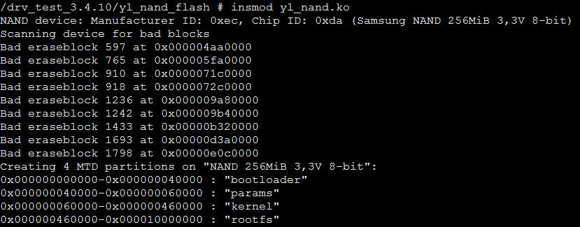
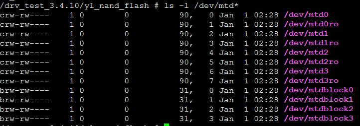
The following device nodes are generated in the device directory: