catalogue
1, Serial port protocol and RS-232 standard
4, Principle of USB/TTL to 232 "module (taking CH340 chip module as an example)
5, Using stm32cubeMX to generate project and burn HEX files through serial port
1, Serial port protocol and RS-232 standard
Serial communication refers to Serial port Sends and receives bytes in bit s byte (byte) serial communication Slow, but the serial port can use one line to send data and another line to receive data at the same time. The serial port communication protocol specifies the contents of the data packet, including the start bit, main data, check bit and stop bit. Both parties need to agree on a consistent data packet format to send and receive data normally. In serial port communication, commonly used protocols include RS-232 and r S-422 and RS-485.
Among them, RS-232 standard interface (also known as EIA RS-232) is commonly used serial communication One of the interface standards, which is composed of American Electronics Industry Association (EIA) United bell systems Modem Manufacturer and computer Terminal manufacturer at 1970 Jointly formulated, its full name is "technical standard for serial binary data exchange interface between data terminal equipment (DTE) and data communication equipment (DCE)".
 rs232 (9-pin) interface
RS-232 bus specifies 25 lines, including two signal channels, namely the first channel (called the main channel) and the second channel (called the sub channel). Full duplex communication can be realized by using RS-232 bus. Generally, the main channel is used, while the sub channel is less used. In general applications, it can be realized by using 3 ~ 9 signal lines Full duplex communication , a simple full duplex communication process can be realized by using three signal lines (receiving line, transmitting line and signal ground).
The standard transmission rates specified by RS-232 include 50b/s, 75b/s, 110b/s, 150b/s, 300b/s, 600b/s, 1200b/s, 2400b/s, 4800b/s, 9600b/s and 19200b/s, which can flexibly adapt to devices with different rates. For slow peripherals, you can choose a lower transmission rate; on the contrary, you can choose a higher transmission rate.
It is specified that the level of logic "1" is - 5V ~ - 15V, and the level of logic "0" is + 5V ~ + 15V. The purpose of selecting this electrical standard is to improve the anti-interference ability and increase the communication distance. The noise tolerance of RS-232 is 2V, and the receiver will recognize the signal as high as + 3V as logic "0" and the signal as low as - 3V as logic "1".
Because RS-232 adopts serial transmission mode, and TTL level When converted to RS-232C level, the transmission distance can generally reach 30 m. if the current loop with photoelectric isolation of 20 mA is used for transmission, the transmission distance can reach 1000 m. In addition, if the Modem is added to the RS-232 bus interface, the transmission distance can be further through wired, wireless or optical fiber.
A connector of RS - 232 interface is the 25 core plug socket of D13 - 25. Generally, the plug is at DCE end and the socket is at DTE end.
There are two kinds of serial port connectors, one is 9-pin serial port (DB-9 for short) and the other is 25 pin serial port (DB-25 for short). Each connector can be divided into male and female. DB9 serial interface is often used in development. Take DB9 as an example, and the following figure shows male and female connectors respectively
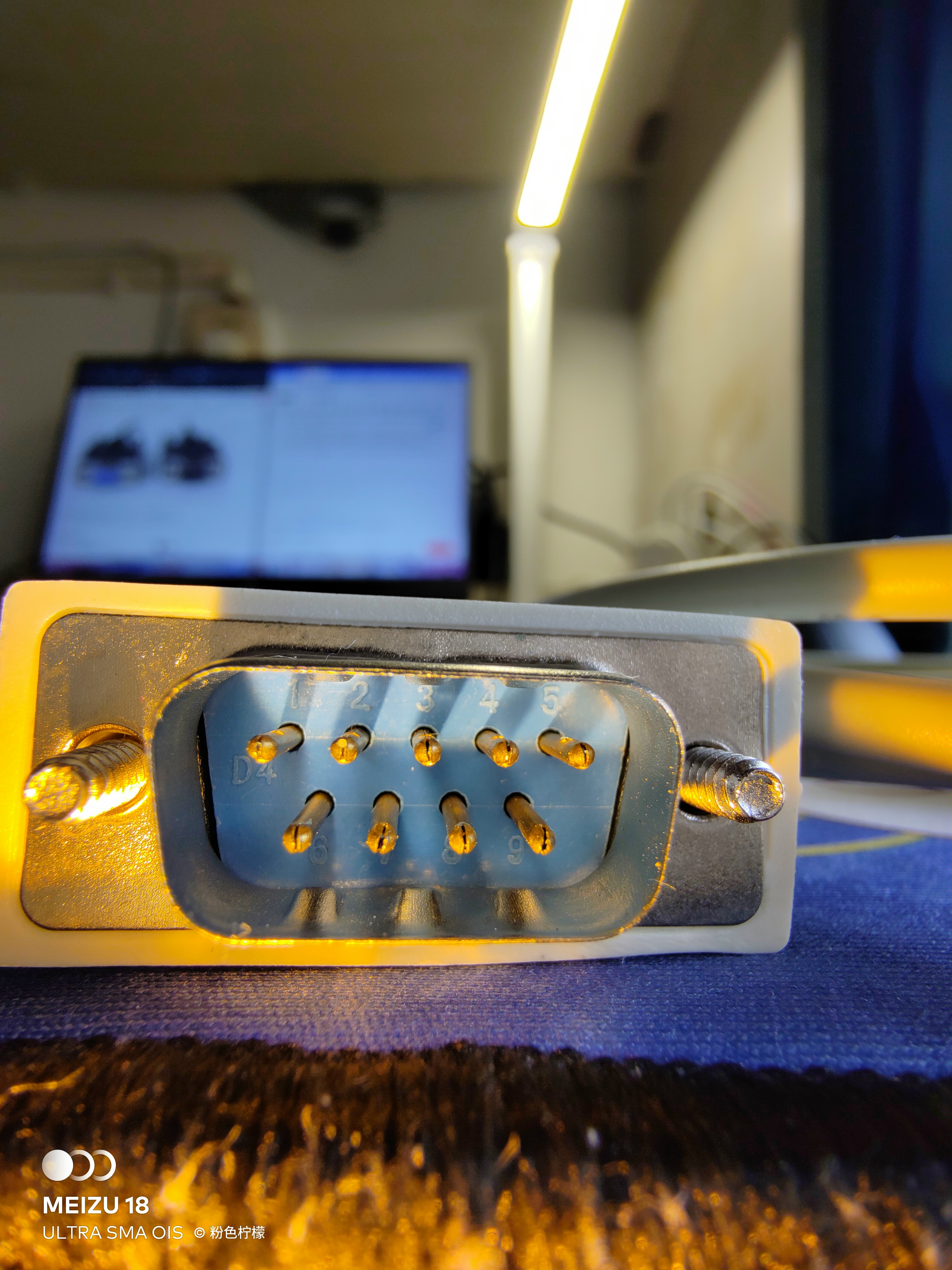 Male head
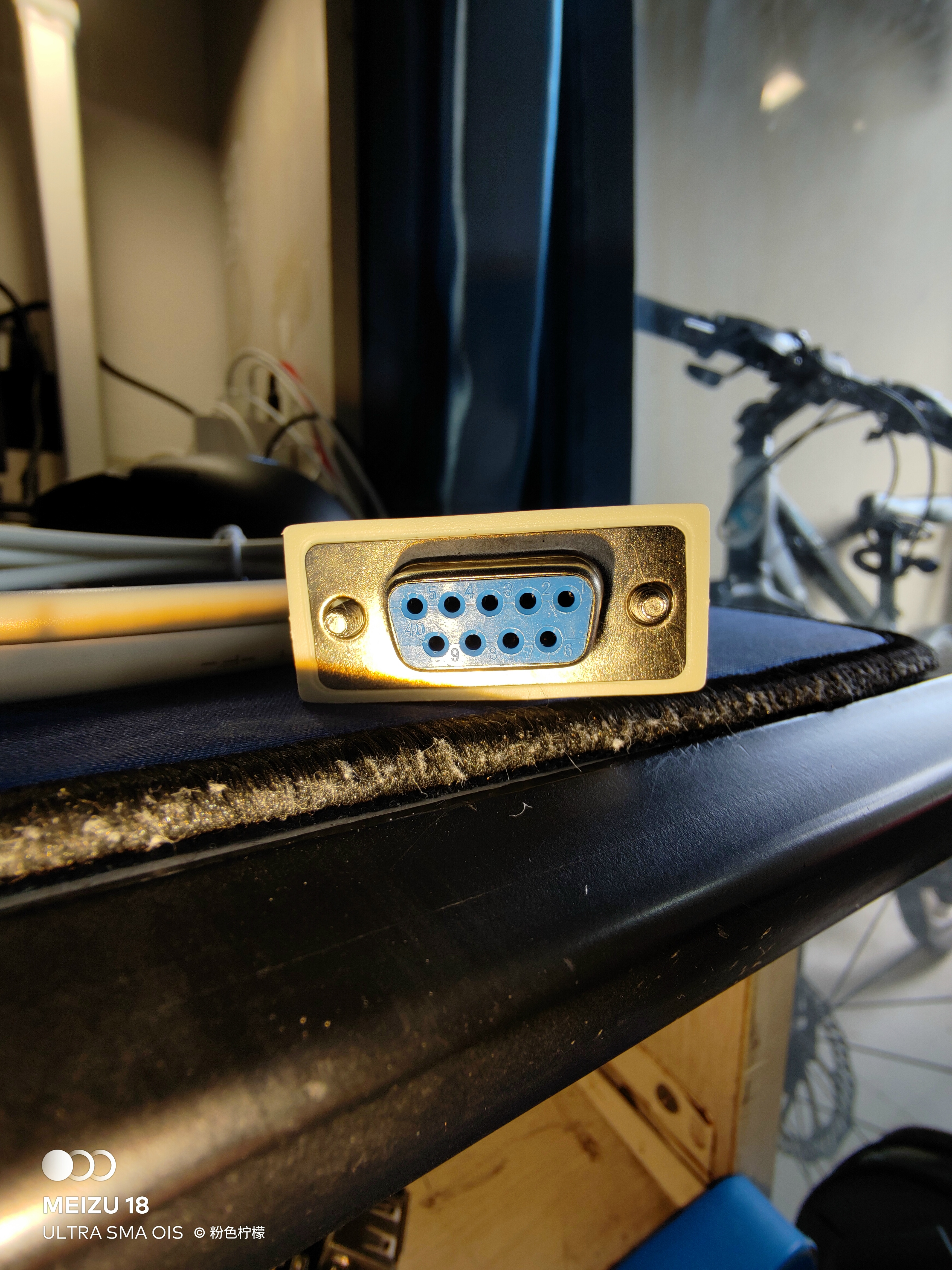 Female head
In the figure, we can see the number of each pin. The following is the description of each pin
1. DCD (Data Carrier Detect): carrier detection. It is mainly used to notify the computer that the Modem is online, that is, the Modem detects a dial tone and is online.
2. RXD (Receive(rx) Data): this pin is used to receive data from external devices; when you use the Modem, you will find that the RXD indicator is flashing, indicating that there is data entry on the RXD pin (2 connected to the RS232 terminal TOUT of MAX232 (such as PIN7)).
3. TXD (Transmit(tx) Data): this pin sends the data of the computer to external devices; when you use the Modem, you will find that the TXD indicator is flashing, indicating that the computer is sending data through the TXD pin.
4. DTR (Data Terminal Ready): the data terminal is ready; when this pin is high, it notifies the Modem that data transmission can be carried out and the computer is ready.
5. GND (Ground): logically.
6. DSR (data set ready): the data setting is ready; when this pin is high, it informs the computer that the Modem is ready for data communication.
7. RTS (Request To Send): Request To Send; this pin is controlled by the computer to inform the Modem to transmit data to the computer immediately; otherwise, the Modem will temporarily put the received data into the buffer.
8. CTS (Clear to send): Clear to send; this pin is controlled by the Modem to inform the computer to send the data to the Modem.
9. RI (Ring Indicator): the Modem notifies the computer of a call coming in. Whether to answer the call is determined by the computer.
2, TTL level
TTL is the abbreviation of transistor transistor logic, which is the standard technology for communication between various parts of equipment controlled by computer processor. TTL level signal is widely used because its data representation adopts binary provisions, + 5V is equivalent to logic "1", and 0V is equivalent to logic "0".
In the digital circuit, the level of the circuit composed of TTL electronic components is a voltage range, which stipulates:
Output high level > = 2.4V, output low level < = 0.4V;
Input high level > = 2.0V, input low level < = 0.8V.
3, RS232 level
On TXD and RXD data lines:
(1) logic 1 is a voltage of - 3~-15V
(2) logic 0 is a voltage of 3~15V
On RTS, CTS, DSR, DTR, DCD and other control lines:
(1) the effective signal (ON state) is 3~15V
(2) the signal is invalid (OFF state) and the voltage is - 3~-15V
This is specified by the communication protocol RS-232.
RS-232: standard serial port, the most commonly used serial communication interface. There are three types (A,B and C), which respectively use different voltages to represent on and off. The most widely used is RS-232C, which defines the voltage of mark(on) bit as - 3V to - 12V, and space(off) The maximum transmission distance is about 15m and the maximum speed is 20kb/s. RS-232 is designed for point-to-point (i.e. only one pair of receiving and transmitting equipment) communication, and its driver load is 3 ~ 7k Ω. Therefore, RS-232 is suitable for communication between local equipment.
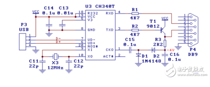
4, Principle of USB/TTL to 232 "module (taking CH340 chip module as an example)
In the figure, it is also a USB to 3-wire RS232 serial port, but the level amplitude of the output RS232 signal is slightly lower. The R232 pin of CH340 is high level, enabling the auxiliary RS232 function, which only needs to be added diode , triode, resistance and capacitance can replace the special level conversion circuit U5 in section 7.2, so the hardware cost is lower.
5, Using stm32cubeMX to generate project and burn HEX files through serial port
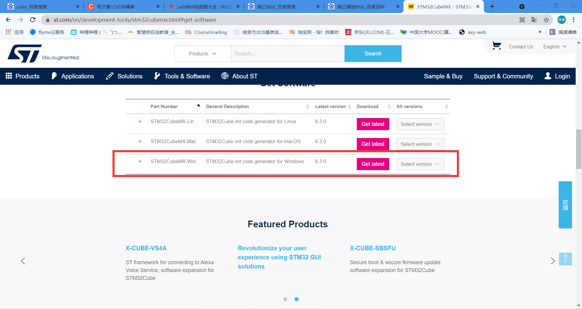
First, install stm32cubeMX, cooperate with Keil, use HAL library to light the LED flow light, that is, use GPIO port to complete the periodic flashing of three LED traffic lights. stm32cubeMX official download link:
https://www.st.com/en/development-tools/stm32cubemx.html#get-software
After entering the link, select the appropriate version to download. My device is windows, so I selected the red box item
After the download is completed, install it. Just follow the installation program. I won't repeat it here
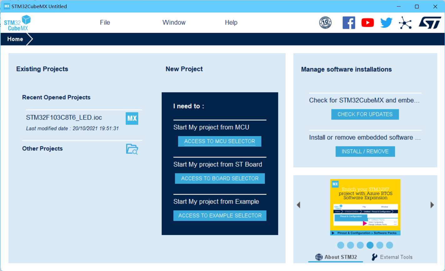
After installation, the following interface is displayed
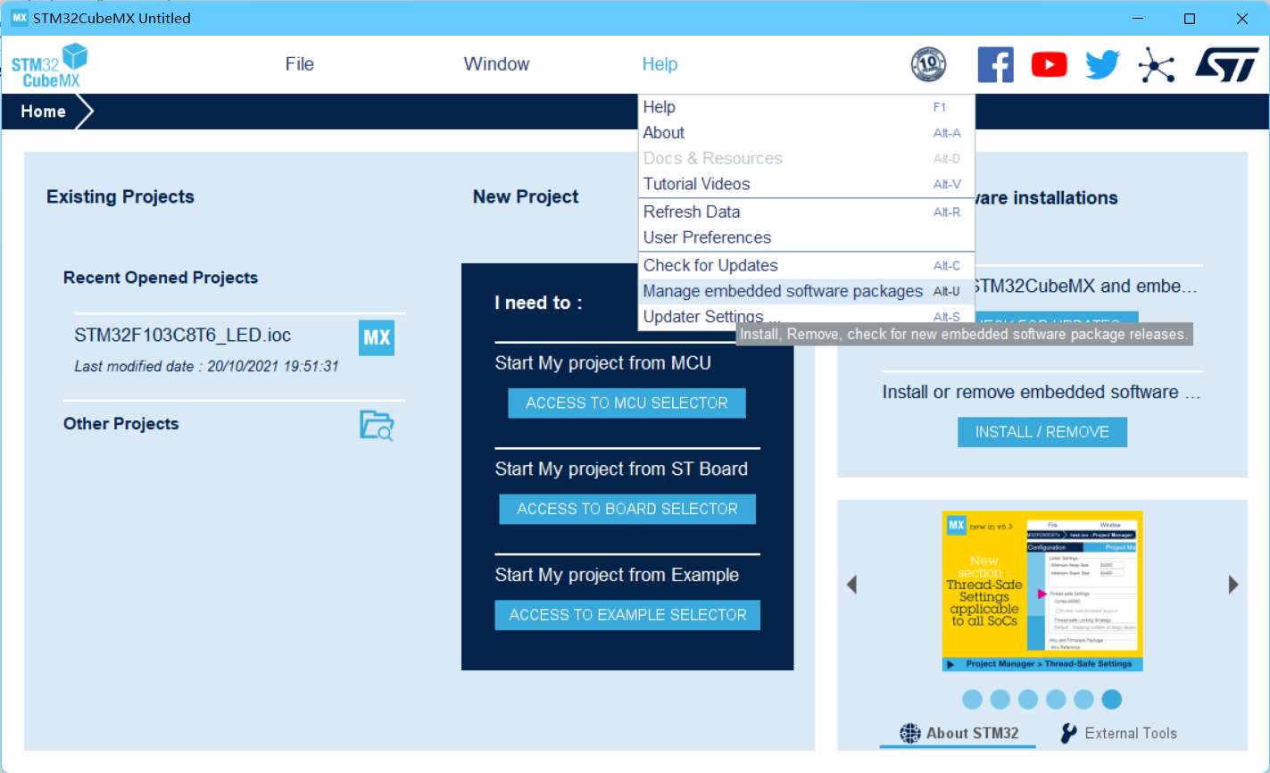
Let's first select manage embedded software packages in help
Then find the corresponding stm32 to download. My stm32f103c8t6, so I chose to download and install the package shown in the red box
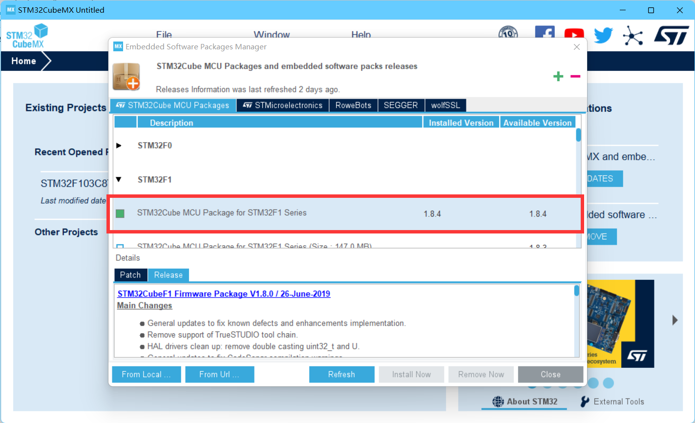
Select and click install now to download and install. After installation, return to the main interface
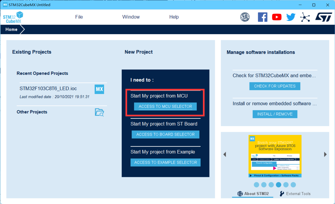
Click on the red box to create a new project
After entering this interface, enter your own chip name in part name to search
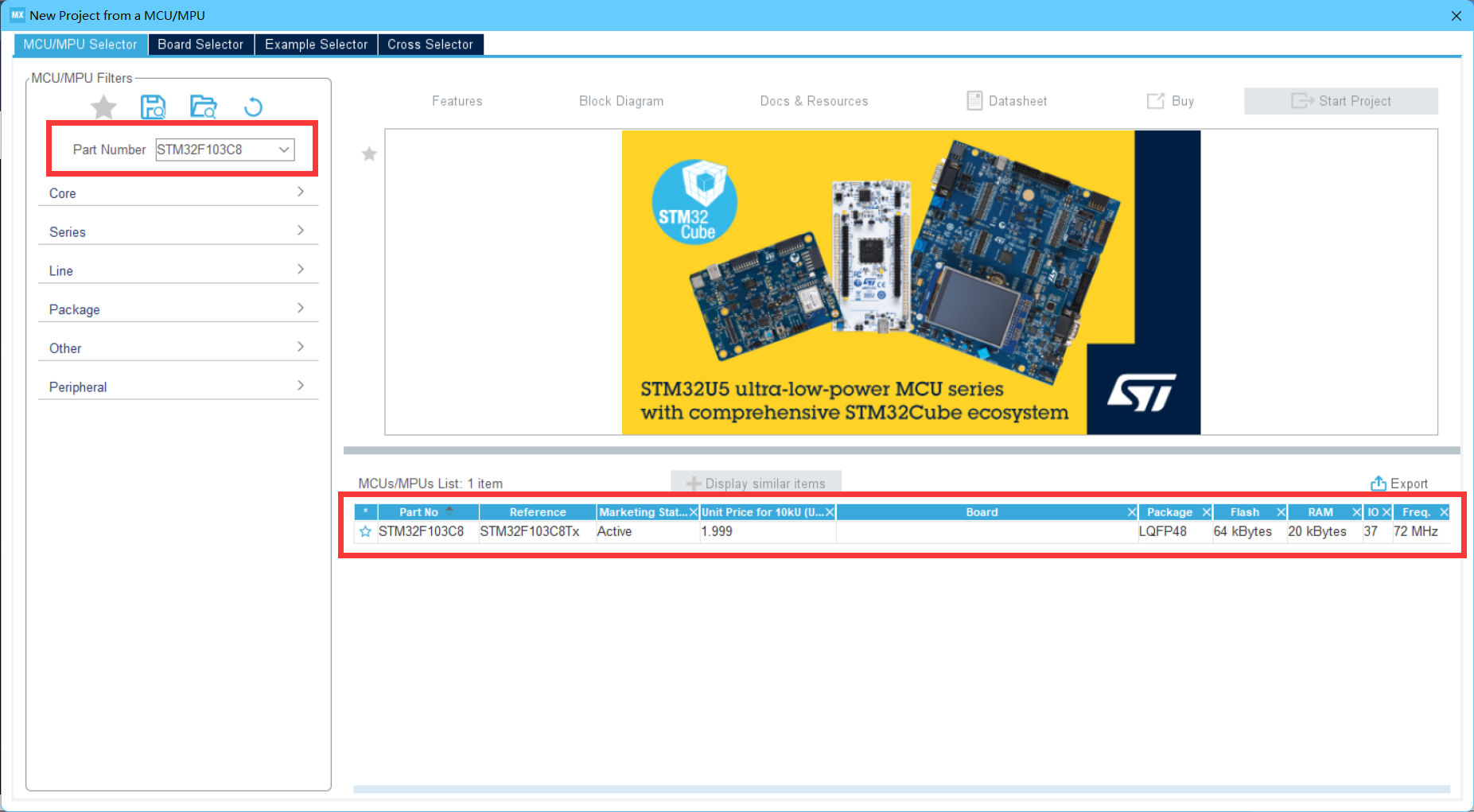
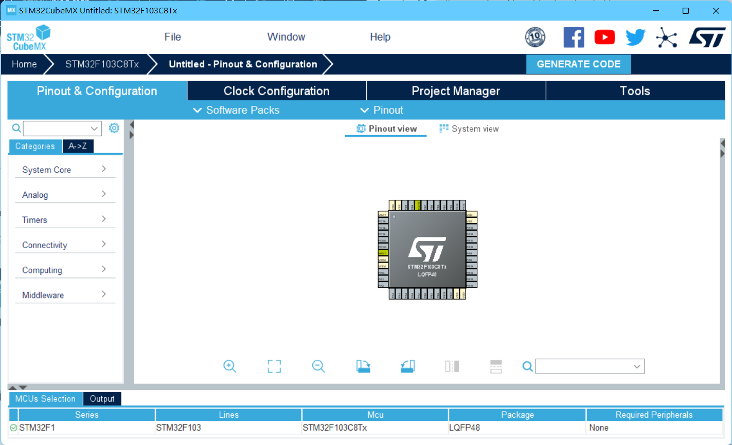
Then select the following information, and finally click start project in the upper right corner to enter the next interface
Click System Core, enter SYS, and select Serial Wire in debug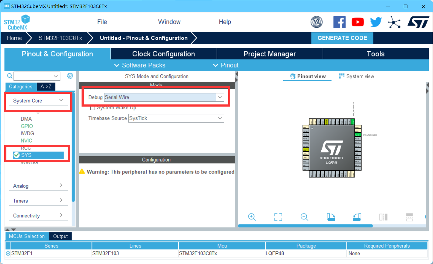
Next, configure the clock, select Clock Configuration, and then select on the right side of PLLCLK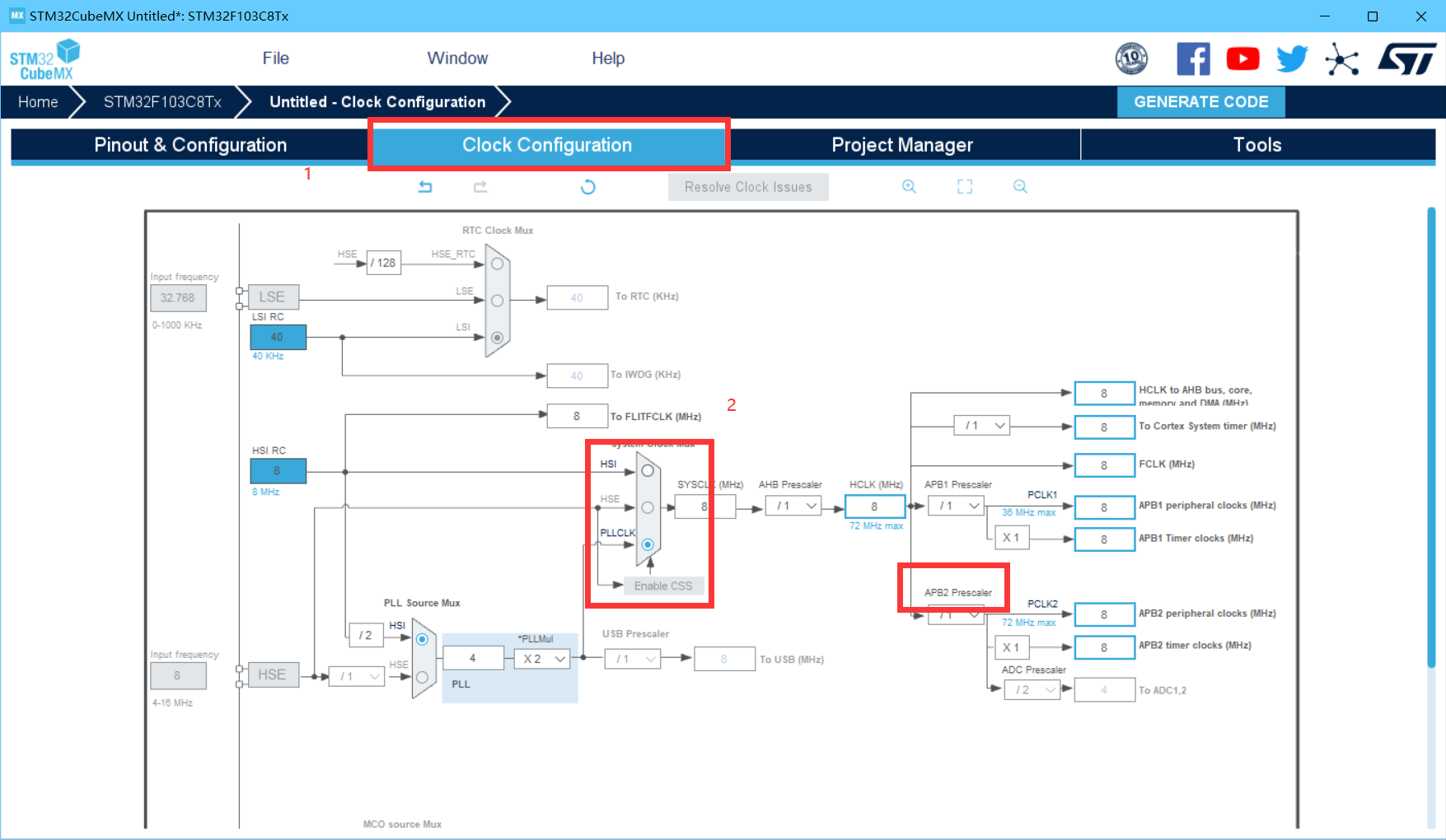
Then return to the previous interface, select RCC, and modify HSE to Crystal/Ceramic Resonator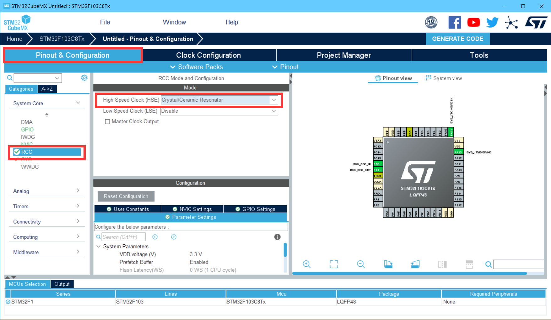
Then we notice the chip diagram on the right
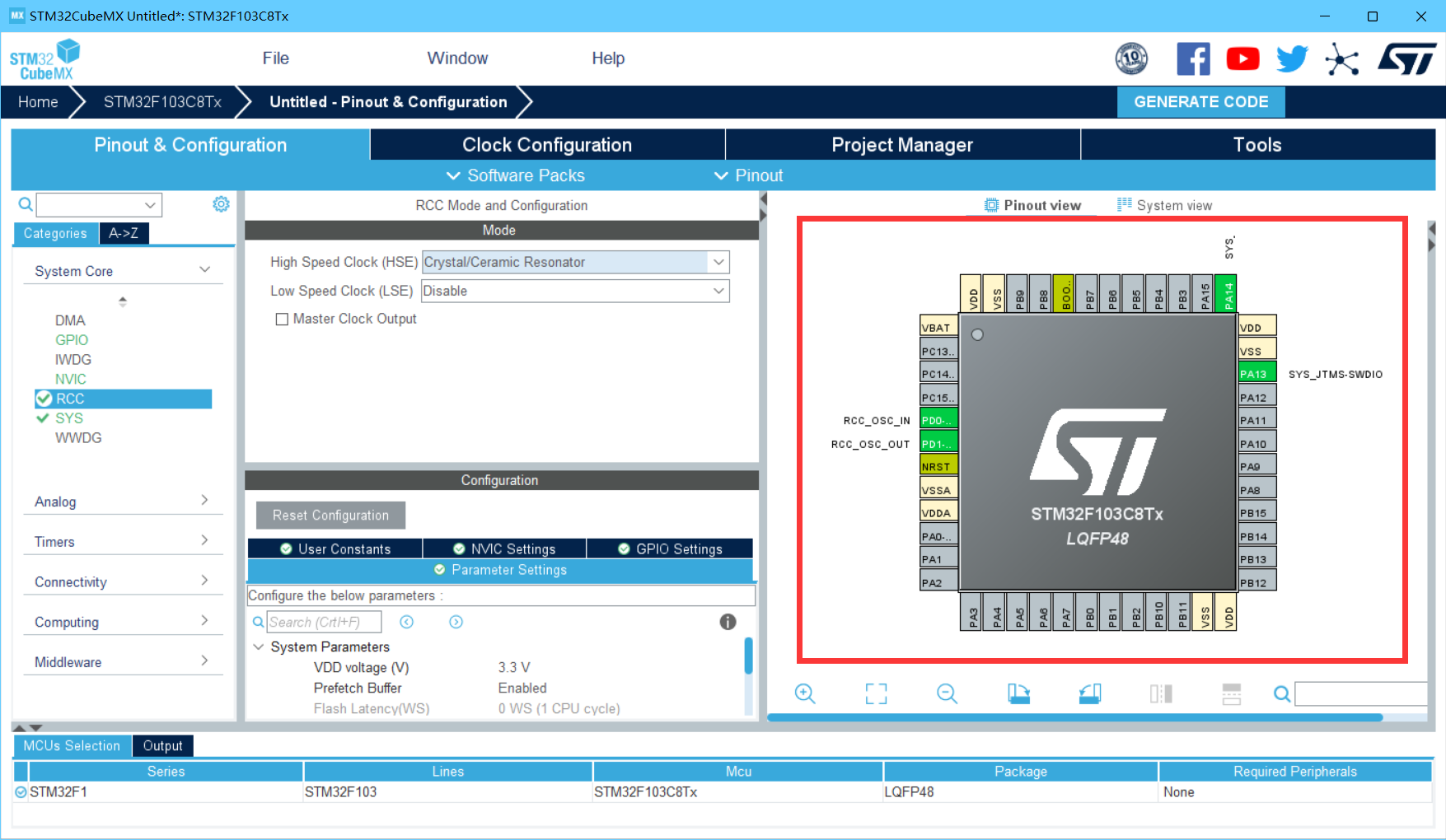
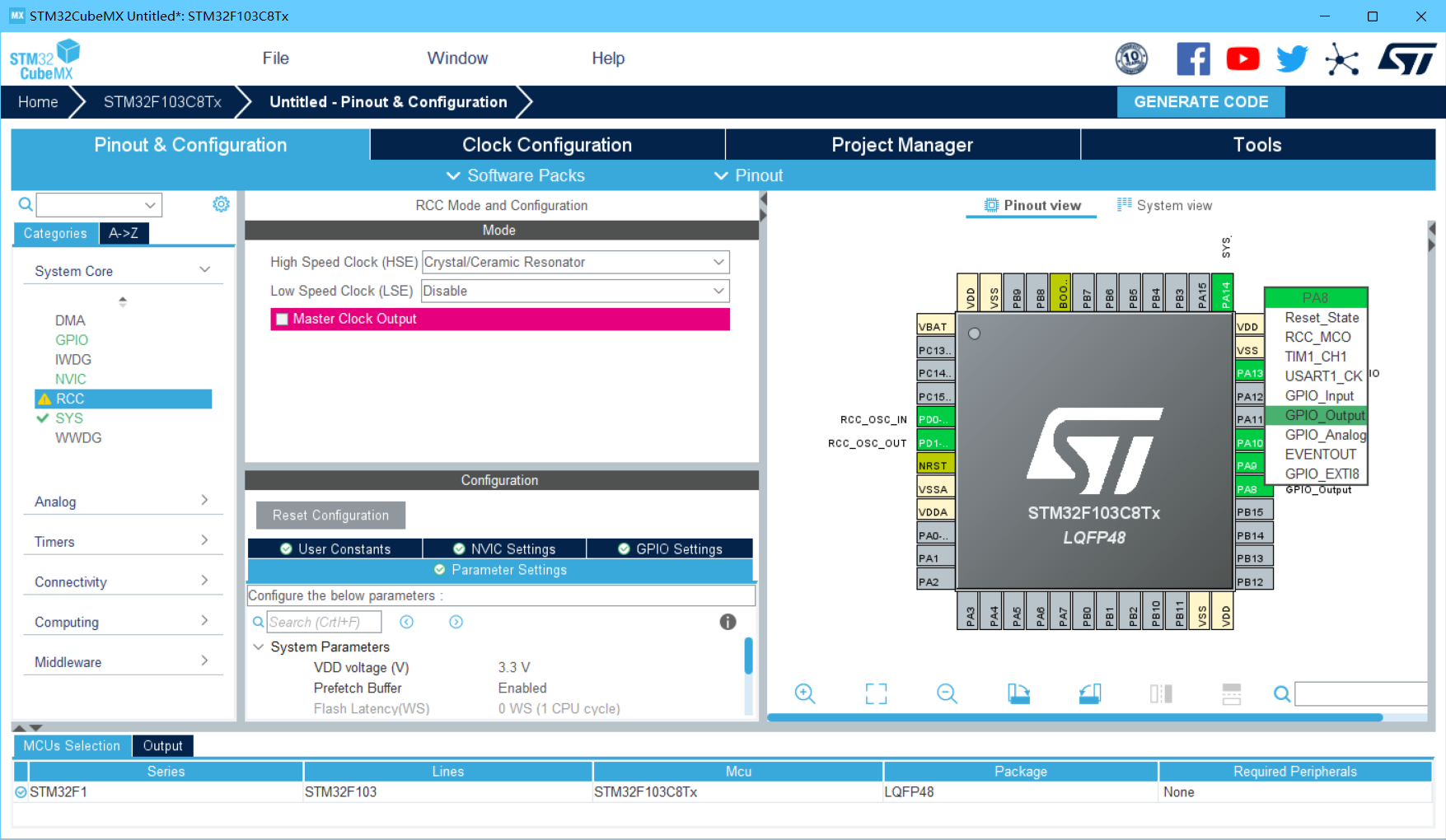
Left click the pin you want to select. I select PA8, PA9 and PA10. Left click and select GPIO_Output
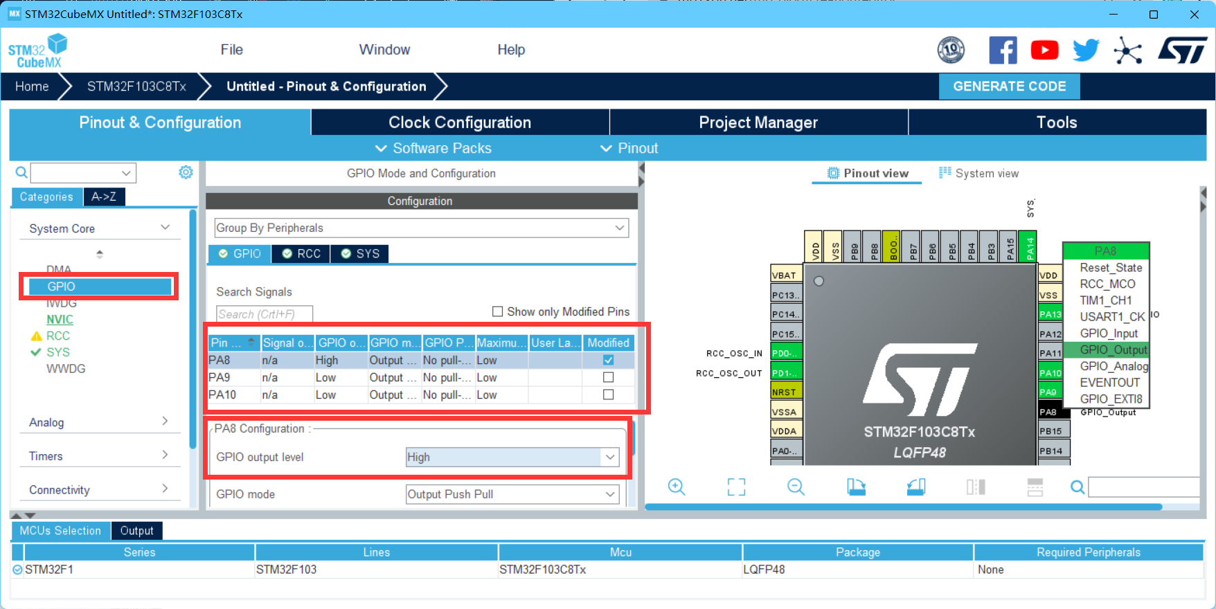
Click GPIO in the System core, click the pin name, and change the output level to high. Note that each pin should be changed (or not)
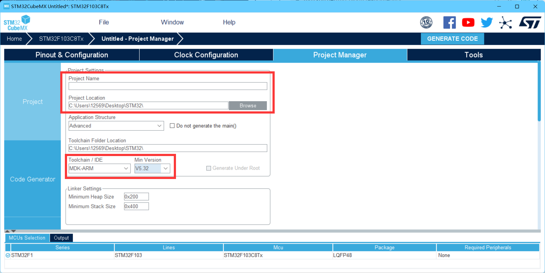
Click project manager, select the path and enter the project name, and then change the IDE to MDK-ARM
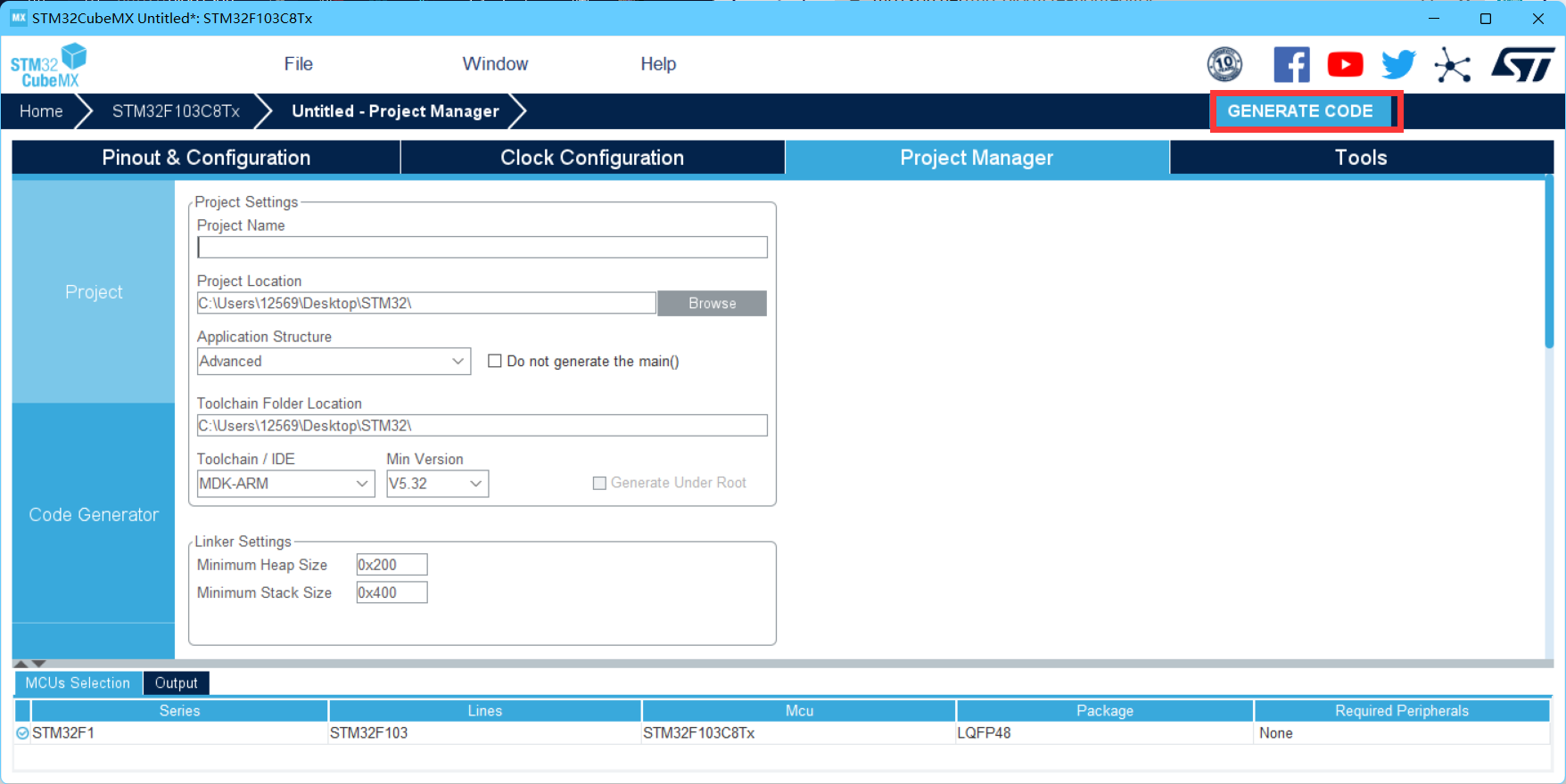
Click GENERATE CODE in the upper right corner to successfully create the project
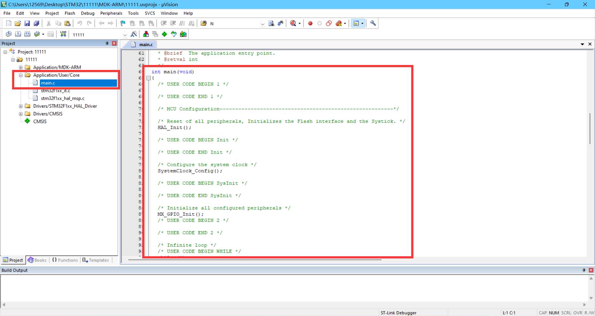
Enter the project target directory set by yourself, open the MDK-ARM folder, open the newly generated project through keil, main.c, and then find the main function
Then put the following code into while
HAL_GPIO_WritePin(GPIOA,GPIO_PIN_8,GPIO_PIN_RESET);
HAL_Delay(1000);
HAL_GPIO_WritePin(GPIOA,GPIO_PIN_8,GPIO_PIN_SET);

HAL_GPIO_WritePin(GPIOA,GPIO_PIN_9,GPIO_PIN_RESET);
HAL_Delay(1000);
HAL_GPIO_WritePin(GPIOA,GPIO_PIN_9,GPIO_PIN_SET);

HAL_GPIO_WritePin(GPIOA,GPIO_PIN_10,GPIO_PIN_RESET);
HAL_Delay(1000);
HAL_GPIO_WritePin(GPIOA,GPIO_PIN_10,GPIO_PIN_SET);
Then burn with serial port. The wiring mode is as follows
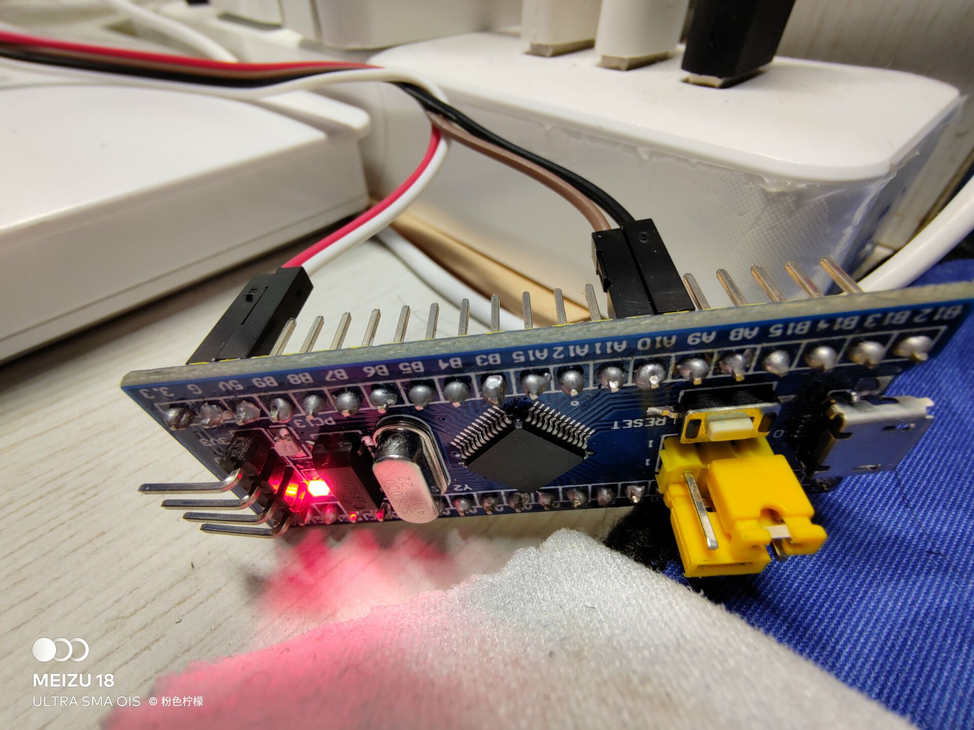
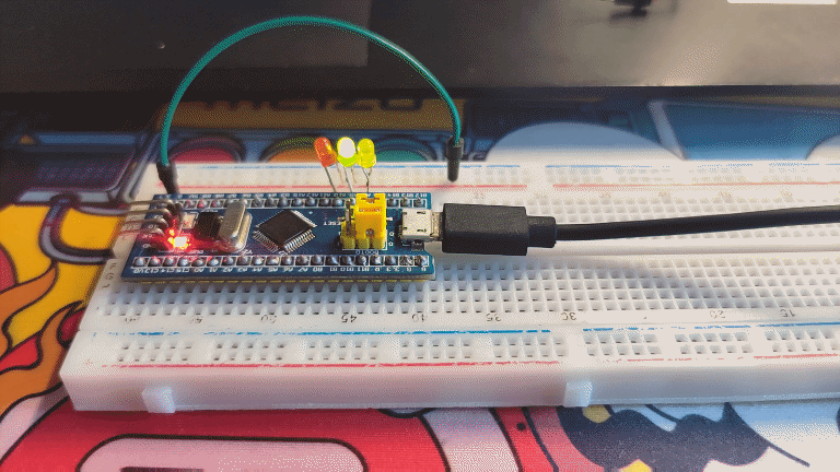
3.3v to 3.3v GND is connected to GND, the module and the serial port pin RX of stm32 correspond to TX, TX corresponds to Rx, that is, A9(TX) is connected to RX pin, A10(RX) is connected to TX pin, and then BOOT0 is modified to 1. The following is the wiring diagram.
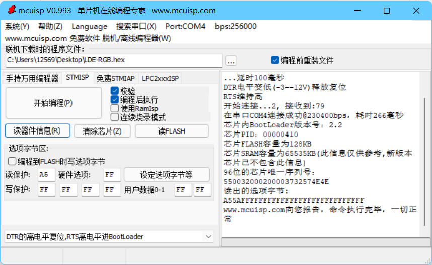
Then enter mcuisp, search the serial port, and click to read the device information. If the connection is successful, it is shown in the figure below
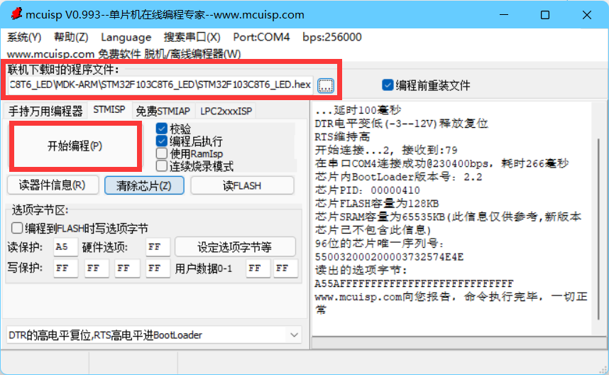
Select hex file and click start programming to start burning
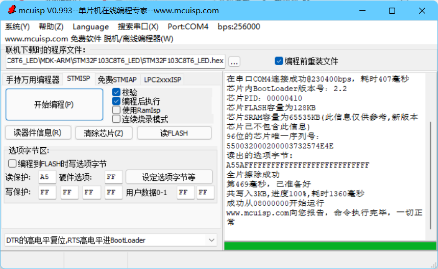
Burning succeeded
Reset BOOT0 to 0. After the bread board is connected to the circuit, it can be powered on. It is found that it runs successfully
In order to explore our delay time, we use keil's own logic analyzer to analyze it
Click the magic wand, and then modify the parameters as shown in the figure below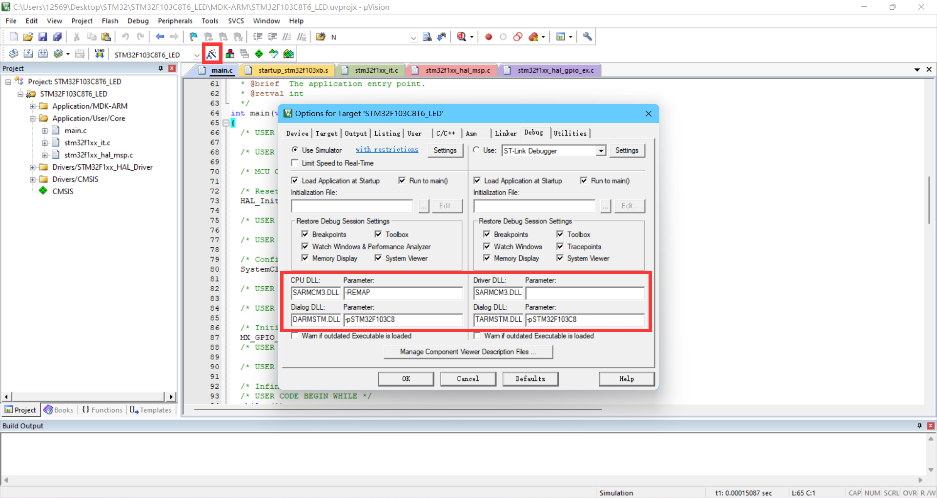
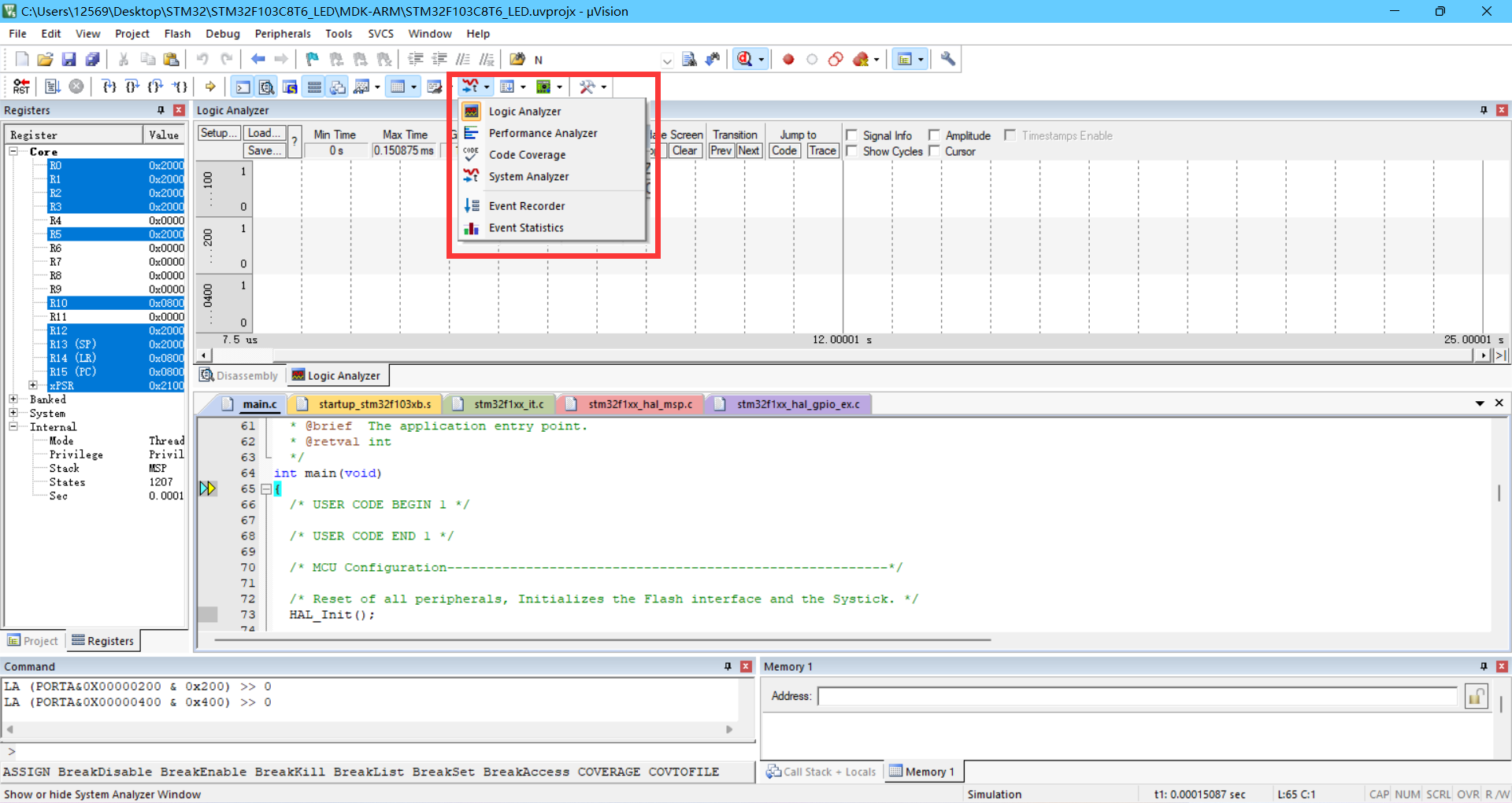
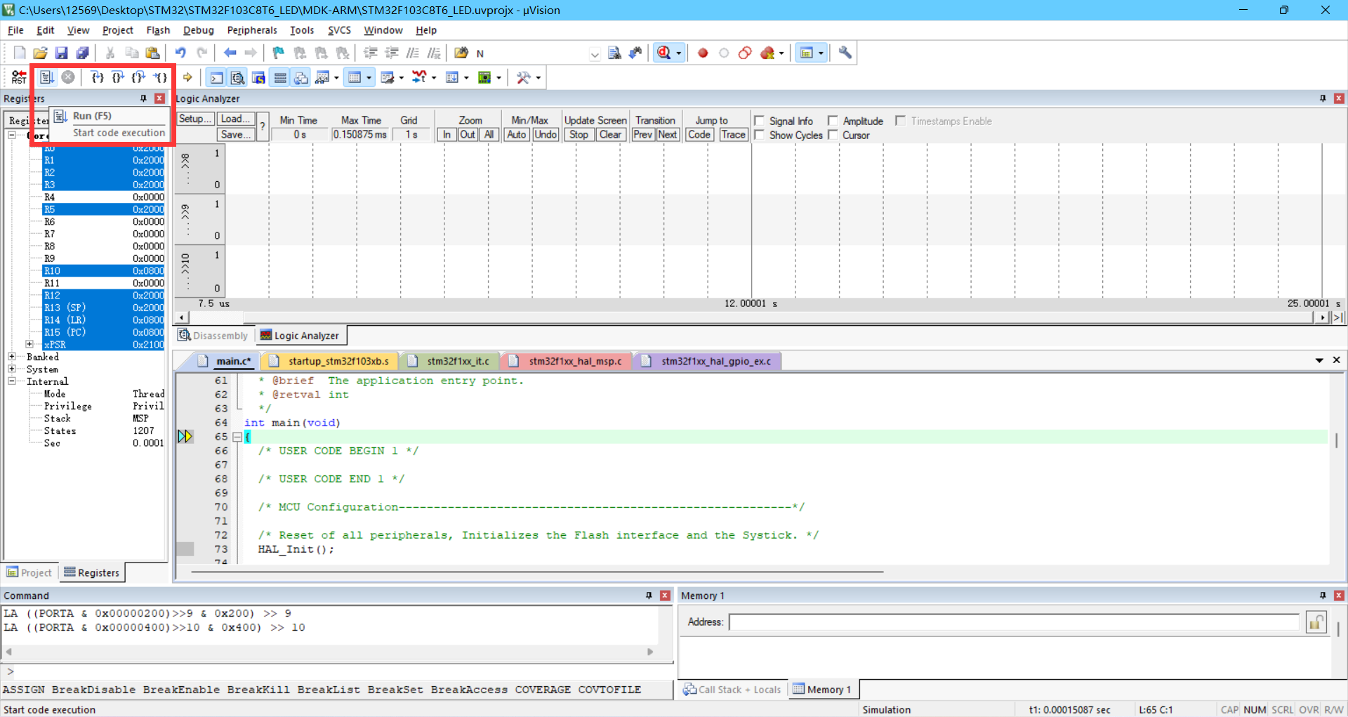
Enter the debug mode, and then open the logic analyzer as shown in the figure
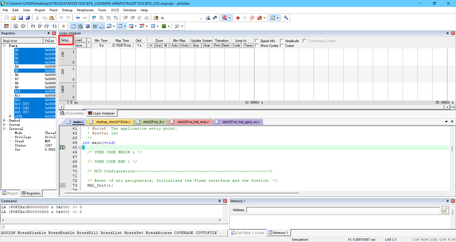
Click setup
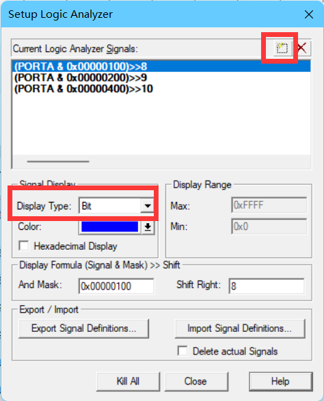
Add the pins to be observed. The selected pins are PA8, PA9 and PA10 respectively. Among them, PORTA is Port A. if it is GPIOB, the corresponding pins should also be written as PORTB and PORTA & After 0x00000100, move 8 bits to the right to obtain the status of PA8. After adding pins, modify the display mode of each pin to Bit
Click run to start running (or directly click F5)
After the program starts running, the effect of logic analyzer is shown in the figure below
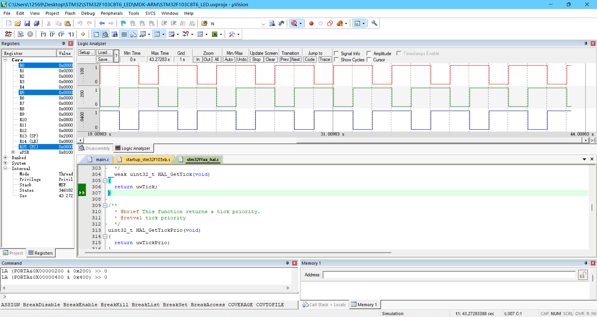
We can easily see that the delay time is 1s
6, Serial communication
Before reference Assembly language engineering simulation and HEX analysis based on stm32f103_ pink_lemon's blog - CSDN blog On this basis, we only need to modify it to create main.s when creating main.c, and then enter the following code
;RCC Register address mapping
RCC_BASE            EQU    0x40021000
RCC_CR              EQU    (RCC_BASE + 0x00)
RCC_CFGR            EQU    (RCC_BASE + 0x04)
RCC_CIR             EQU    (RCC_BASE + 0x08)
RCC_APB2RSTR        EQU    (RCC_BASE + 0x0C)
RCC_APB1RSTR        EQU    (RCC_BASE + 0x10)
RCC_AHBENR          EQU    (RCC_BASE + 0x14)
RCC_APB2ENR         EQU    (RCC_BASE + 0x18)
RCC_APB1ENR         EQU    (RCC_BASE + 0x1C)
RCC_BDCR            EQU    (RCC_BASE + 0x20)
RCC_CSR             EQU    (RCC_BASE + 0x24)

;AFIO Register address mapping
AFIO_BASE           EQU    0x40010000
AFIO_EVCR           EQU    (AFIO_BASE + 0x00)
AFIO_MAPR           EQU    (AFIO_BASE + 0x04)
AFIO_EXTICR1        EQU    (AFIO_BASE + 0x08)
AFIO_EXTICR2        EQU    (AFIO_BASE + 0x0C)
AFIO_EXTICR3        EQU    (AFIO_BASE + 0x10)
AFIO_EXTICR4        EQU    (AFIO_BASE + 0x14)

;GPIOA Register address mapping
GPIOA_BASE          EQU    0x40010800
GPIOA_CRL           EQU    (GPIOA_BASE + 0x00)
GPIOA_CRH           EQU    (GPIOA_BASE + 0x04)
GPIOA_IDR           EQU    (GPIOA_BASE + 0x08)
GPIOA_ODR           EQU    (GPIOA_BASE + 0x0C)
GPIOA_BSRR          EQU    (GPIOA_BASE + 0x10)
GPIOA_BRR           EQU    (GPIOA_BASE + 0x14)
GPIOA_LCKR          EQU    (GPIOA_BASE + 0x18)

;GPIO C Mouth control
GPIOC_BASE          EQU    0x40011000
GPIOC_CRL           EQU    (GPIOC_BASE + 0x00)
GPIOC_CRH           EQU    (GPIOC_BASE + 0x04)
GPIOC_IDR           EQU    (GPIOC_BASE + 0x08)
GPIOC_ODR           EQU    (GPIOC_BASE + 0x0C)
GPIOC_BSRR          EQU    (GPIOC_BASE + 0x10)
GPIOC_BRR           EQU    (GPIOC_BASE + 0x14)
GPIOC_LCKR          EQU    (GPIOC_BASE + 0x18)

;Serial port 1 control
USART1_BASE         EQU    0x40013800
USART1_SR           EQU    (USART1_BASE + 0x00)
USART1_DR           EQU    (USART1_BASE + 0x04)
USART1_BRR          EQU    (USART1_BASE + 0x08)
USART1_CR1          EQU    (USART1_BASE + 0x0c)
USART1_CR2          EQU    (USART1_BASE + 0x10)
USART1_CR3          EQU    (USART1_BASE + 0x14)
USART1_GTPR         EQU    (USART1_BASE + 0x18)

;NVIC Register address
NVIC_BASE           EQU    0xE000E000
NVIC_SETEN          EQU    (NVIC_BASE + 0x0010)
;SETENA Starting address of register array
NVIC_IRQPRI         EQU    (NVIC_BASE + 0x0400)
;Start address of interrupt priority register array
NVIC_VECTTBL        EQU    (NVIC_BASE + 0x0D08)
;Address of vector table offset register
NVIC_AIRCR          EQU    (NVIC_BASE + 0x0D0C)
;Address of application interrupt and reset control register
SETENA0             EQU    0xE000E100
SETENA1             EQU    0xE000E104


;SysTick Register address
SysTick_BASE        EQU    0xE000E010
SYSTICKCSR          EQU    (SysTick_BASE + 0x00)
SYSTICKRVR          EQU    (SysTick_BASE + 0x04)

;FLASH Buffer register address image
FLASH_ACR           EQU    0x40022000

;SCB_BASE           EQU    (SCS_BASE + 0x0D00)

MSP_TOP             EQU    0x20005000
;Starting value of main stack
PSP_TOP             EQU    0x20004E00
;Process stack start value

BitAlias_BASE       EQU    0x22000000
;Bit alias area start address
Flag1               EQU    0x20000200
b_flas              EQU    (BitAlias_BASE + (0x200*32) + (0*4))
;Bit address
b_05s               EQU    (BitAlias_BASE + (0x200*32) + (1*4))
;Bit address
DlyI                EQU    0x20000204
DlyJ                EQU    0x20000208
DlyK                EQU    0x2000020C
SysTim              EQU    0x20000210


;Constant definition
Bit0                EQU    0x00000001
Bit1                EQU    0x00000002
Bit2                EQU    0x00000004
Bit3                EQU    0x00000008
Bit4                EQU    0x00000010
Bit5                EQU    0x00000020
Bit6                EQU    0x00000040
Bit7                EQU    0x00000080
Bit8                EQU    0x00000100
Bit9                EQU    0x00000200
Bit10               EQU    0x00000400
Bit11               EQU    0x00000800
Bit12               EQU    0x00001000
Bit13               EQU    0x00002000
Bit14               EQU    0x00004000
Bit15               EQU    0x00008000
Bit16               EQU    0x00010000
Bit17               EQU    0x00020000
Bit18               EQU    0x00040000
Bit19               EQU    0x00080000
Bit20               EQU    0x00100000
Bit21               EQU    0x00200000
Bit22               EQU    0x00400000
Bit23               EQU    0x00800000
Bit24               EQU    0x01000000
Bit25               EQU    0x02000000
Bit26               EQU    0x04000000
Bit27               EQU    0x08000000
Bit28               EQU    0x10000000
Bit29               EQU    0x20000000
Bit30               EQU    0x40000000
Bit31               EQU    0x80000000


;Vector table
    AREA RESET, DATA, READONLY
    DCD    MSP_TOP            ;Initialize main stack
    DCD    Start              ;Reset vector
    DCD    NMI_Handler        ;NMI Handler
    DCD    HardFault_Handler  ;Hard Fault Handler
    DCD    0
    DCD    0
    DCD    0
    DCD    0
    DCD    0
    DCD    0
    DCD    0
    DCD    0
    DCD    0
    DCD    0
    DCD    0
    DCD    SysTick_Handler    ;SysTick Handler
    SPACE  20                 ;Reserved space 20 bytes


;Code snippet
    AREA |.text|, CODE, READONLY
    ;Main program start
    ENTRY
    ;Instructs the program to execute from here
Start
    ;Clock system settings
    ldr    r0, =RCC_CR
    ldr    r1, [r0]
    orr    r1, #Bit16
    str    r1, [r0]
    ;Enable external crystal oscillator
    ;Start external 8 M Crystal oscillator

ClkOk
    ldr    r1, [r0]
    ands   r1, #Bit17
    beq    ClkOk
    ;Wait for the external crystal oscillator to be ready
    ldr    r1,[r0]
    orr    r1,#Bit17
    str    r1,[r0]
    ;FLASH Buffer
    ldr    r0, =FLASH_ACR
    mov    r1, #0x00000032
    str    r1, [r0]

    ;set up PLL The PLL magnification is 7,HSE Input no frequency division
    ldr    r0, =RCC_CFGR
    ldr    r1, [r0]
    orr    r1, #(Bit18 :OR: Bit19 :OR: Bit20 :OR: Bit16 :OR: Bit14)
    orr    r1, #Bit10
    str    r1, [r0]
    ;start-up PLL Phase locked loop
    ldr    r0, =RCC_CR
    ldr    r1, [r0]
    orr    r1, #Bit24
    str    r1, [r0]
PllOk
    ldr    r1, [r0]
    ands   r1, #Bit25
    beq    PllOk
    ;choice PLL Clock as system clock
    ldr    r0, =RCC_CFGR
    ldr    r1, [r0]
    orr    r1, #(Bit18 :OR: Bit19 :OR: Bit20 :OR: Bit16 :OR: Bit14)
    orr    r1, #Bit10
    orr    r1, #Bit1
    str    r1, [r0]
    ;other RCC Related settings
    ldr    r0, =RCC_APB2ENR
    mov    r1, #(Bit14 :OR: Bit4 :OR: Bit2)
    str    r1, [r0]


    ;IO port settings
    ldr    r0, =GPIOC_CRL
    ldr    r1, [r0]
    orr    r1, #(Bit28 :OR: Bit29)
    ;PC.7 Output mode,Maximum speed 50 MHz
    and    r1, #(~Bit30 & ~Bit31)
    ;PC.7 Universal push-pull output mode
    str    r1, [r0]

    ;PA9 Serial port 0 transmitting pin
    ldr    r0, =GPIOA_CRH
    ldr    r1, [r0]
    orr    r1, #(Bit4 :OR: Bit5)
    ;PA.9 Output mode,Maximum speed 50 MHz
    orr    r1, #Bit7
    and    r1, #~Bit6
    ;10: Multiplexing function push-pull output mode
    str    r1, [r0]


    ldr    r0, =USART1_BRR
    mov    r1, #0x271
    str    r1, [r0]
    ;Configure baud rate-> 115200

    ldr    r0, =USART1_CR1
    mov    r1, #0x200c
    str    r1, [r0]
    ;USART Module total enable send and receive enable
    ;71 02 00 00   2c 20 00 00

    ;AFIO Parameter setting
    ;Systick Parameter setting
    ldr    r0, =SYSTICKRVR
    ;Systick Initial installation value
    mov    r1, #9000
    str    r1, [r0]
    ldr    r0, =SYSTICKCSR
    ;set up,start-up Systick
    mov    r1, #0x03
    str    r1, [r0]

    ;NVIC
    ;ldr   r0, =SETENA0
    ;mov   r1, 0x00800000
    ;str   r1, [r0]
    ;ldr   r0, =SETENA1
    ;mov   r1, #0x00000100
    ;str   r1, [r0]

    ;Switch to user level line program mode
    ldr    r0, =PSP_TOP
    ;Initialize thread stack
    msr    psp, r0
    mov    r0, #3
    msr    control, r0

    ;initialization SRAM register
    mov    r1, #0
    ldr    r0, =Flag1
    str    r1, [r0]
    ldr    r0, =DlyI
    str    r1, [r0]
    ldr    r0, =DlyJ
    str    r1, [r0]
    ldr    r0, =DlyK
    str    r1, [r0]
    ldr    r0, =SysTim
    str    r1, [r0]

;Main cycle
main
    ldr    r0, =Flag1
    ldr    r1, [r0]
    tst    r1, #Bit1
    ;SysTick Generate 0.5s,Set bit 1
    beq    main                  ;0.5s The flag is not set yet

    ;0.5s The flag has been set
    ldr    r0, =b_05s
    ;Bit band operation reset 0.5s sign
    mov    r1, #0
    str    r1, [r0]
    bl     LedFlas


    mov    r0, #'H'
    bl     send_a_char

	mov    r0, #'e'
    bl     send_a_char

	mov    r0, #'l'
    bl     send_a_char

	mov    r0, #'l'
    bl     send_a_char

	mov    r0, #'o'
    bl     send_a_char

	mov    r0, #' '
    bl     send_a_char

	mov    r0, #'w'
    bl     send_a_char

	mov    r0, #'o'
    bl     send_a_char

	mov    r0, #'r'
    bl     send_a_char

	mov    r0, #'l'
    bl     send_a_char

	mov    r0, #'d'
    bl     send_a_char

	mov    r0, #'\n'
    bl     send_a_char

	b      main


;Subroutine serial port 1 sends a character
send_a_char
    push   {r0 - r3}
    ldr    r2, =USART1_DR
    str    r0, [r2]
b1
    ldr    r2, =USART1_SR
    ldr    r2, [r2]
    tst    r2, #0x40
    beq    b1
    ;Send complete(Transmission complete)wait for
    pop    {r0 - r3}
    bx     lr


;subroutine led twinkle
LedFlas
    push   {r0 - r3}
    ldr    r0, =Flag1
    ldr    r1, [r0]
    tst    r1, #Bit0
    ;bit0 Flashing flag bit
    beq    ONLED        ;Open for 0 led lamp
    ;Off for 1 led lamp
    ldr    r0, =b_flas
    mov    r1, #0
    str    r1, [r0]
    ;The flashing flag position is 0,The next status is on
    ;PC.7 Output 0
    ldr    r0, =GPIOC_BRR
    ldr    r1, [r0]
    orr    r1, #Bit7
    str    r1, [r0]
    b      LedEx
ONLED
    ;Open for 0 led lamp
    ldr    r0, =b_flas
    mov    r1, #1
    str    r1, [r0]
    ;The flashing flag position is 1,The next status is off
    ;PC.7 Output 1
    ldr    r0, =GPIOC_BSRR
    ldr    r1, [r0]
    orr    r1, #Bit7
    str    r1, [r0]
LedEx
    pop    {r0 - r3}
    bx     lr

;Abnormal program
NMI_Handler
    bx     lr


HardFault_Handler
    bx     lr

SysTick_Handler
    ldr    r0, =SysTim
    ldr    r1, [r0]
    add    r1, #1
    str    r1, [r0]
    cmp    r1, #500
    bcc    TickExit
    mov    r1, #0
    str    r1, [r0]
    ldr    r0, =b_05s
    ;The clock tick counter is set to 0 when it is greater than or equal to 500 times of clearing.5s Flag bit
    ;Bit band operation set 1
    mov    r1, #1
    str    r1, [r0]
TickExit
    bx     lr

    ALIGN
    ;By using zero or null instructions NOP fill,Aligns the current position with a specified boundary
    END
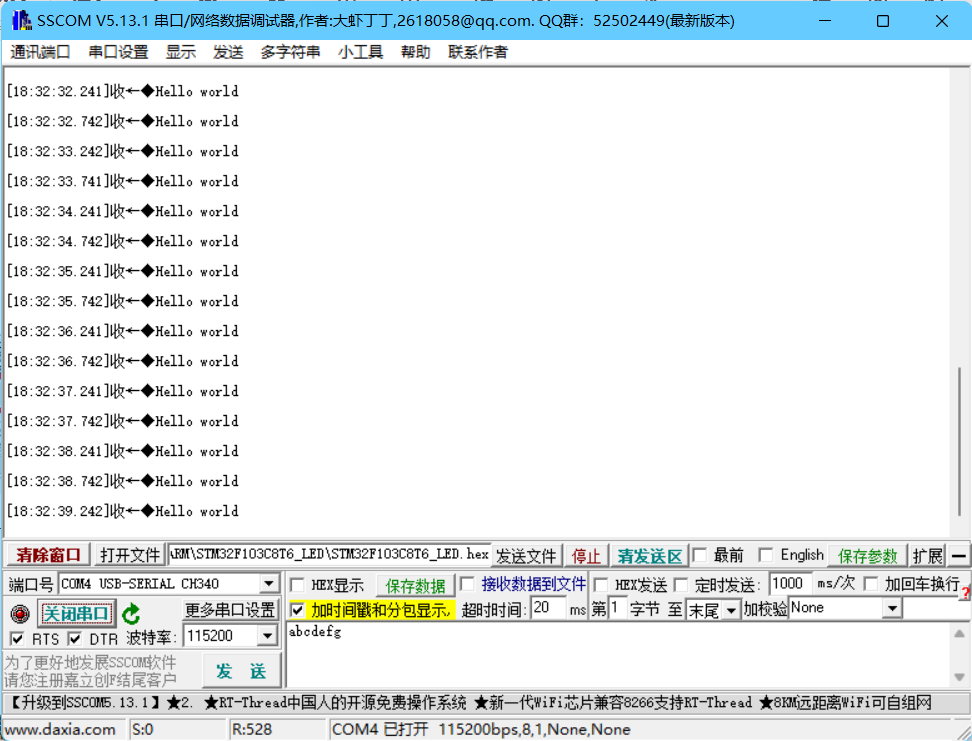
After compiling the project, burn the hex file into stm32. Refer to the above for the burning process. After burning, do not change the wiring mode, modify the boot0 to 0 position, and open the serial communication debugger
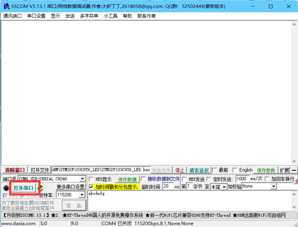
The final effect is as follows
7, Summary
Understand the serial port protocol, learn how to burn hex files through the serial port, learn how to use keil5's own logic analyzer to analyze the pin output waveform, so as to analyze whether the project runs successfully, and learn how to carry out serial port communication. The code and operation are not complicated, but the process is slightly cumbersome, so you need to calm down and learn
8, References
https://blog.csdn.net/m0_38022615/article/details/81293880
http://www.elecfans.com/emb/jiekou/20180511676053.html
https://blog.csdn.net/junseven164/article/details/120807138?spm=1001.2014.3001.5501