Experiment 8: nixie tube display experiment
1. Experimental purpose
- Learn the basic principle of "seven section common cathode nixie tube" display;
- Master the method of controlling multiple nixie tube displays through parallel interface chip.
2. Experimental content
Use port A and port B of an 8255 interface chip to connect the digital tube segment code interface (ABCDEFG Dp) and bit code interface (X1~X6) respectively. Write A program to realize the following two display modes:
- Make the six digit nixie tube display the moving numbers 0 to 9 bit by bit from right to left, that is, the number 0 moves from the rightmost end to the leftmost end, the number 1 moves from the rightmost end to the leftmost end,..., and the number 9 moves from the rightmost end to the leftmost end, and cycle the above process;
- Make the six digit nixie tube display the stable number "123456" from left to right.
3. Experimental principle
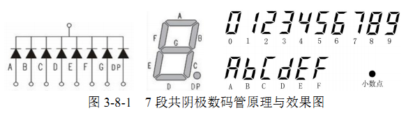
The schematic diagram and display effect of 7-segment common cathode nixie tube are shown in figure 3-8-1, including 7 strokes A ~ G and a decimal point Dp. The 7-segment common cathode nixie tube displays 0 ~ 9, A ~ F, and its codes are 3FH, 06H, 5BH, 4FH, 66H, 6DH, 7DH, 07H, 7FH, 6FH, 77H, 7CH, 39H, 5EH, 79H and 71H. When the decimal point "." is displayed, the highest bit on the current code is set to 1 (80H). The available code 00H is off, or the set selection signal is invalid.
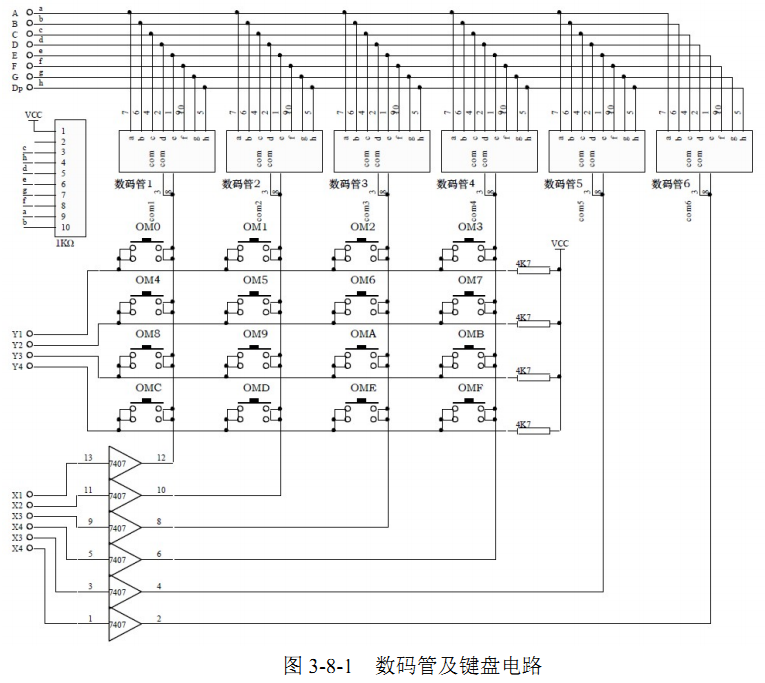
The circuit and external interface of six digit nixie tube are shown in figure 3-9-1. The specific nixie tube can be selected and lit through the bit selection signal (X1~X6), and the specific number can be displayed through the input segment code (ABCDEFG Dp). When multiple digits are displayed at the same time, the bit code can be scanned.
4. Experimental records
-
Bit selection signal: there are 6 nixie tubes on the machine. You can select which nixie tubes the segment selection signal is output to through ports X1 ~ X6. It can be seen from the circuit diagram that when X1 ~ X6 ports output 1, it is not selected, and when 0 is output, it is selected.
-
Segment selection signal: there are 8 segments of LED lights in the nixie tube. The corresponding LED lights are on and off by inputting 8-bit binary digital selection control. Input 1 to control on, and input 0 to control off.
-
Display problem: each time another nixie tube is selected, the original lit nixie tube will be extinguished because its bit selection signal is set to 0 and the bit selection signal of the other nixie tube is set to high. So we should write six nixie tubes in a six cycle, and an external dead cycle to make the six nixie tubes always on.
-
Experiment 1: cyclic shift display 0 to 9
A8255 EQU 0640H		;8255 Port A Address of
B8255 EQU 0642H		;8255 Port B Address of
C8255 EQU 0644H		;8255 Port C Address of
M8255 EQU 0646H		;8255 Control address of
DATA SEGMENT
TAB:
	DB 3FH,06H,5BH,4FH,66H,6DH,7DH,07H,7FH,6FH
DATA ENDS
CODE SEGMENT
	ASSUME CS:CODE,DS:DATA
START:
	MOV AX,DATA
	MOV DS,AX		;These two lines can DATA Data import using
	MOV DX,M8255
	MOV AL,80H
	OUT DX,AL		;Set the control mode of 8255 as ABC All ports output
	LEA BX,TAB		;deposit TAB First address of
	MOV SI,00H		;Address offset
MAIN:
	MOV AL,11011111B	;Initial setting of bit code selection, select the nixie tube at the rightmost end
	MOV CX,06H			;set up LOOP The number of cycles is 6
M1:
	MOV DX,A8255
	OUT DX,AL			;First output bit selection through 8255
	SHR AL,1			;Shift the bit selection one bit to the right
	OR AL,11000000B		;Due to the right shift and zero filling, you need to manually change 0 to 1

	PUSH AX				;preservation AX Value of
	MOV DX,B8255
	MOV AL,[BX+SI]		;TAB First address+Address offset
	OUT DX,AL			;Output segment code selection through 8255
	POP AX				;Take out the saved AX Value of

	CALL DELAY		;A delay is required
	LOOP M1			;LOOP Loop, return M1 Tag bit

	INC SI			;If the address offset increases, the segment selection code of the next number will be selected
	CMP SI,0AH		;Detect whether the offset is out of range
	JNE M1F			;Jump without crossing the boundary
	MOV SI,00H		;Set zero when crossing the boundary
M1F:
	JMP MAIN

DELAY:			;A visible delay, about 3/10 Seconds or so
	PUSH BX
	PUSH CX
	MOV BX, 0003H
	DEL2: MOV CX, 0FFFFH
	DEL3: LOOP DEL3
		DEC BX
	JNZ DEL2
	POP CX
	POP BX
	RET
CODE ENDS
	END START
- Experiment 2: stably display numbers 1 ~ 6 (only important codes are recorded here because some codes are repeated)
	LEA BX,TAB			;deposit TAB First address of
MAIN2:
	MOV AL,11011111B	;Bit code selection initial setting
	MOV SI,00H			;Address offset
	MOV CX,06H			;set up LOOP Number of cycles
M2:
	MOV DX,A8255
	OUT DX,AL			;First input the bit selection code
	SHR AL,1			;Bit selection right shift
	OR AL,11000000B

	PUSH AX
	MOV DX,B8255
	MOV AL,[BX+SI]		;Re output segment code selection
	OUT DX,AL
	POP AX

	INC SI			;Auto increment offset, select the next number
	CALL DELAY		;A short delay is required
	LOOP M2			;LOOP loop

	JMP MAIN2

DELAY:				;A short delay
	PUSH BX
	MOV BX, 01FFH
	DEL:
		DEC BX
		JNZ DEL
	POP BX
	RET
5. Extended experiment
No, no code.