Theory and design of single-stage CIC filter
- Project brief
- Multi rate signal processing
- CIC filter
- FPGA implementation of CIC filter
- CIC decimation filter code
- CIC decimation filter test code
- Simulation results of CIC decimation filter
- CIC interpolation filter code
- CIC interpolation filter test code
- Simulation results of CIC interpolation filter
- reference
- summary
Project brief
If you want to do well in your work, you must first sharpen your tools. Signal processing has a strong theoretical support. If you don't master these theories and just look for some code that meets the requirements, it's hard to get closer. And the algorithm itself is the difficulty of FPGA engineers, not the hardware logic. Therefore, in this paper, we will design CIC anti aliasing filter, which plays an important role in signal processing. Next, we will explain CIC design from two aspects of theory and FPGA design
Multi rate signal processing
This concept is relative to Single Rate signal processing. Single Rate means that there is only one data rate in the whole signal processing flow; multi rate means that there are multiple data rates in the system. The use of multi rate signal processing can save storage space, reduce the amount of communication data, reduce the amount of calculation, and reduce the difficulty of design.
Obviously, it can be understood literally that multiple sampling rates are multiple sampling rates. The FIR and IIR filters mentioned above have only one sampling frequency, which is a fixed sampling rate. However, in some cases, signals with different sampling frequencies are needed. For specific examples, we will take digital down conversion (DDC) as an example to explain.
According to the traditional rate conversion theory, we want to realize the conversion of sampling rate. We can do this. If there is a useful sine wave analog signal, the AD sampling rate is f1. Now I need to use the signal whose sampling frequency is f2. The traditional method is to DA convert the signal sampled by f1, and then sample the converted analog signal with f2 sampling frequency The digital signal with sampling rate of f2 is obtained, and the conversion of sampling frequency is completed. So we introduce a better extraction and interpolation method.
For example, in DDC (digital down conversion) system, the front stage needs a high sampling rate fs to ensure the signal-to-noise ratio of the signal collected by the ADC; after de carrier and extracting the low-frequency baseband signal, the effective bandwidth of the signal has been very small, and the sampling rate that can meet the requirements at this time is far lower than FS. If the processing of data rate conversion is not carried out, it will cause a lot of waste of resources and design problems Difficulties:
Multi rate signal processing includes data rate conversion and LPF design. Data rate conversion includes Decimation (reduce sampling rate) and interpolation (increase sampling rate). In the process of Decimation / interpolation, it should be ensured that there is no spectrum aliasing in the effective frequency band of the signal, so it is necessary to complete the design of LPF, including multi rate FIR filter, CIC filter and HB filter.
From the above article, we can see that the most important operation of multi rate filter is the two operations of * * decimation * * and * * interpolation * *.
extract
When it is necessary to reduce the sampling rate, the input signal data is taken every D-1, and the extracted data is sorted in turn. This process is called d-times extraction, and the sampling rate becomes the original 1/D. However, we need to ensure that the sampling rate after extraction can still meet Nyquist sampling theorem, otherwise it will cause spectrum aliasing. Of course, since the conversion of ADC will also introduce white noise in the whole frequency band, it is necessary to add anti aliasing filter before decimation. As shown in the figure below:
The above is the main operation of extraction, which is also the operation of most FPGA engineers, but they do not understand the principle. Next, we will explain the above two points from the perspective of signal processing:
1. Why do we have to ensure that the Nyquist sampling theorem is satisfied after extraction.
2. Why go through anti aliasing filter first.
First, let's explain the meaning of ××××××××××××××××××××××××××××××××××××××××××××××××××××××××××××××××××××××××××××××××××××××××××××××××××××××××××××××××××××××××××××××× Is it equivalent to that I used 1 / 5 times the sampling frequency of f1 to sample the analog signal? Therefore, the process of sampling is to reduce the sampling rate, but we know that this is the sampling in the time domain. The sampling in the time domain is equal to the periodic extension of the signal waveform in the frequency domain (the formula in the signal system), and the period is the sampling frequency. Therefore, in order to avoid the generation of spectrum aliasing in the frequency domain, the sampling theorem is also the factor we should consider
Let's introduce in detail: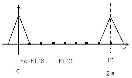
As shown in the figure above, if the above is the frequency spectrum of a useful signal sampled by the sampling frequency f1, assuming that the sampling frequency is 8Khz at this time, it can be obtained through the number lattice. There are eight spaces from 0 to F1, each of which represents 1Khz. Some friends may ask, isn't this in the digital frequency domain? Isn't the unit π? Where is the hz? Yes, here is the digital frequency domain. The sampling frequency f1 corresponds to 2 π. Here is just for good explanation. We use the analog frequency to correspond to the digital frequency (if we don't understand here, we need to supplement the knowledge of signal system and digital signal processing).
The following figure shows the sampling frequency of F1 of 1 / 5 times of the signal. It can be seen that due to the occurrence of spectrum aliasing, because F1 of 1 / 5 times of the signal is 1600hz, and the frequency band of the signal is 1000hz, which does not meet the sampling theorem, leading to the occurrence of spectrum aliasing. Therefore, in order to avoid this situation, in addition to meeting the sampling theorem, that is, the sampling multiple cannot be too high, we also need to Set the frequency band of the signal below F1/2 to ensure that the signal does not have spectrum aliasing. Therefore, we need to add a low-pass filter before decimation, which is called anti aliasing low-pass filter in the book, to limit the frequency band of the signal, and then decimation.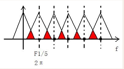
In this case, let's calculate that the cut-off frequency of the low-pass filter is 1 / 2 times the sampling rate after decimation, that is, fc = 1/2 * (F1/M), and M is the decimation multiple. The frequency of 1/2*F1 is π, so we get that the cut-off frequency of anti aliasing low-pass filter is π / m.
Interpolation
When the sampling rate needs to be increased, ***I-1 zero values * * * are inserted between two adjacent data, and then low-pass filtering is carried out. This process is called I times interpolation, and the sampling rate becomes the original I times. As long as the passband of LPF is the effective bandwidth of signal, even if only zero value points (points without sampling values) are inserted during interpolation, the effect of I-fold interpolation can be achieved. The output of the interpolated signal from DAC will introduce less high frequency noise. As shown in the figure below:
The process of extraction is to reduce the sampling rate, so the process of interpolation is to improve the sampling rate. The general idea can be understood in this way. We interpolate every two points of the digital signal obtained by f1 sampling. The inserted value is 0. After interpolation, the number of sampling points of the signal increases in unit time, which is, of course, the increase of sampling rate. After the increase of sampling rate, we know that the number of cycles of the signal spectrum will increase: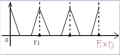
Good students of signal system can try to deduce the above spectrum changes, I believe it is not too difficult.
It should be noted that before and after the interpolation, we only inserted a D-1 zero value in the middle of the time domain signal, which only changed the sampling rate, and did not change the signal information. Therefore, in the frequency domain, the shape of the signal spectrum will not change, only the correspondence between the analog frequency and the digital frequency, as shown in the figure above, F1 is the sampling frequency of the signal before the interpolation, and the interpolation After the value, the shape of the signal spectrum remains unchanged, the sampling frequency becomes * * F1D, and D is the interpolation multiple. If we directly use F1D times of sampling rate to collect signals, we will find that there will be no middle two waveforms, so these two waveforms are redundant, which is called mirror spectrum * in the book. Since it is redundant, we can filter it out with a low-pass filter. Such a low-pass filter is called a mirror low-pass filter. So let's calculate the cutoff frequency of the image lowpass filter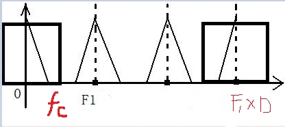
According to the above figure, we can find the cut-off frequency of the image low-pass filter. It can be seen that fc = 1/2 F1, Here we assume that the sampling frequency after interpolation is F2 =F1D, then fc =1/2*(F2/D), while 1/2F2 corresponds to π. Note that 1/2F2 corresponds to π, not 1/2*F1, because this is the spectrum after the sampling rate increases after interpolation, so we get that the cutoff frequency of image low-pass filter is π / d
Fractional multiple extraction and interpolation
The above extraction and interpolation realize the conversion of integer multiple data rate. However, the actual design will not encounter more integer multiple relationships. We can use interpolation and extraction to complete the data rate conversion of the ratio of the sampling rate to the rational number, and we can share one LPF, and we can select the minimum bandwidth of the two cut-off frequencies. As shown in the figure below:
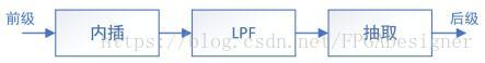
According to the previous introduction of extraction and interpolation, we know that the process of interpolation is to carry out interpolation first, and then through the image low-pass filter. The process of extraction is to carry out anti aliasing low-pass filter first, and then extract. We can see that if we want to carry out fractional multiple extraction, for example, if we want to carry out 3 / 5-fold extraction, we can carry out 3-fold interpolation first, and then 5-fold extraction In this way, fractional multiple extraction can be realized.
Again, when fractional decimation and interpolation are carried out, the image low-pass filter and anti aliasing low-pass filter are connected together, so we can combine the two filters into one, and the cut-off frequency is the minimum value of the cut-off frequency of the two filters.
The above knowledge about data extraction and interpolation has been introduced. If you don't understand anything, you can refer to book knowledge. From this article we can also see the importance of the theoretical knowledge of digital signal processing. If the students in university read this article, here we exhort them to learn the basic theory well, otherwise, they can only be a transfer participant.
CIC filter
CIC filter is a common module of wireless communication, which is generally used in digital down conversion (DDC) and digital up conversion (DUC) systems. CIC filter has simple structure, no multiplier, only adder, integrator and register, which can realize high-speed filtering, * * * is often used in the first stage with the highest input sampling rate. From the above we can see the advantages of CIC filter: CIC (Cascaded Integrator Comb) integral comb filter and other multi rate FIR filter have the advantages of fast operation speed, low resource consumption and high working frequency (because CIC only uses adders, subtracters and registers), which are more widely used in multi rate signal processing system.
Theoretical derivation of CIC filter
Single stage CICI filter
CIC filter consists of two basic parts: integral part and dressing part, as shown in the figure: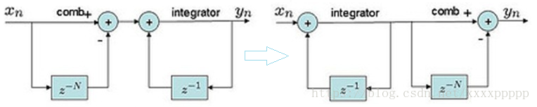
The integrator of the integral part is a unipolar IIR filter with a feedback coefficient of 1 and a state equation of:
y ( n ) = y ( n − 1 ) + x ( n ) y(n)=y(n−1)+x(n) y(n)=y(n−1)+x(n)
The integrator mentioned above can also be regarded as an accumulator. According to Z-transform, the transfer function of integrator is:
H 1 ( z ) = 1 1 − z − 1 H_1(z)=\frac{1}{1−z^{-1}} H1(z)=1−z−11
The dresser is a FIR filter, and its state equation is:
y ( n ) = x ( n − 1 ) − x ( n − D M ) y(n)=x(n−1)-x(n−DM) y(n)=x(n−1)−x(n−DM)
Where D is the design parameter, called differential delay, and its transfer function is:
H c ( z ) = 1 − z − D M H_c(z)=1−z^{-DM} Hc(z)=1−z−DM
Then: the transfer function of the single-stage CIC filter is:
H ( z ) = 1 1 − z − 1 ( 1 − z D M ) H(z)=\frac{1}{1−z^{-1}}(1−z^{DM}) H(z)=1−z−11(1−zDM)
Let z = E J W z = e {JW} z = ejw, and bring it into the above formula, we can get the amplitude frequency response of the transfer function as follows: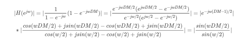
The amplitude frequency response characteristics of CIC filter are shown in the figure, in which [0,2 π / DM] is the main lobe and other intervals are called side lobes.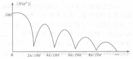
It can be seen from the amplitude frequency response characteristics that the maximum value of the main lobe is DM (at w=0), and the maximum value of the side lobe is obtained at w = 3 π / DM w=3 π / DM w=3 π / DM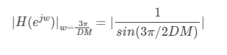
Its ratio to the main lobe level is:
According to θ ≈ s i n θ ≈ sin θ ≈ sin θ at θ 0 ~ 45 °, we can get:
α = 20 l g ( 3 π 2 ) = 13.36 d B α=20lg(\frac{3π}{2})=13.36dB α=20lg(23π)=13.36dB
It can be seen that the sidelobe level of single-stage CIC filter is large and the stopband attenuation is poor. In order to reduce the sidelobe level, the cascade method of multi-stage CIC filter can be used.
Multistage CICI filter
According to the above, the first sidelobe level attenuation of the single-stage CIC filter is fixed at 13.46dB, which is independent of the order of the filter. This value does not meet the normal requirements of stopband attenuation. The solution is to achieve larger stopband attenuation by cascading CIC filters. In fact, in practical application, multi-stage CIC filter is used.
The transfer function of an N-level CIC decimation filter system is:
H ( z ) = ( 1 − z − D M 1 − z − 1 ) N H(z)=(\frac{1−z^{−DM}}{1−z^{−1}})^N H(z)=(1−z−11−z−DM)N
In the N-stage cascade, the stopband attenuation is N times of the single-stage attenuation, i.e. 13.46 × N(dB).
However, in the case of stopband attenuation, there are also a series of problems:
1. It is difficult to realize CIC filter which can meet the error of pass band tolerance and stop band tolerance at the same time, because if the stop band attenuation is large, the filter series must be increased, but the pass band tolerance will be increased.
2. If such a filter is to be implemented, only when the frequency band of the useful signal is very small relative to the rate of the sampling signal can a filter be designed to meet the requirements. In this way, if the passband attenuation is large, the effect on the useful signal is small.
3. The frequency band of useful signal is very small compared with the sampling signal, which means the sampling rate of signal is very high. Therefore, CIC filter is suitable for the front-end of multi rate signal processing, as anti aliasing filter, or as anti aliasing interpolation filter at the back-end.
FPGA implementation of CIC filter
We have described the main principles of CIC. In fact, CIC filter is a simple low-pass filter in essence. It is only convenient to connect with decimation and interpolation. Here we will give the source code for you to learn:
CIC decimation filter code
The 50 MHz sampling rate is used to sample the 0.25 MHz signal, and the sampling rate is reduced to 10 MHz by 5 times of the fifth-order CIC filter. Here we give the CIC decimation filter code directly,
cic module:
`timescale 1ns / 1ps
// *********************************************************************************
// Project Name : OSXXXX
// Author       : zhangningning
// Email        : nnzhang1996@foxmail.com
// Website      :
// Module Name  : cic.v
// Create Time  : 2020-04-24 15:08:16
// Editor       : sublime text3, tab size (4)
// CopyRight(c) : All Rights Reserved
//
// *********************************************************************************
// Modification History:
// Date             By              Version                 Change Description
// -----------------------------------------------------------------------
// XXXX       zhangningning          1.0                        Original
//
// *********************************************************************************

module cic(
    //System Interfaces
    input                   sclk            ,
    input                   rst_n           ,
    //Communication Interfaces
    input                   rvalid          ,
    input           [ 9:0]  din             ,
    output  reg             tvalid          ,
    output  reg     [12:0]  dout
);

//========================================================================================\
//**************Define Parameter and  Internal Signals**********************************
//========================================================================================/
reg                 [ 2:0]  cnt             ;
reg                 [12:0]  sum             ;
wire                [12:0]  din_x           ;


//========================================================================================\
//**************     Main      Code        **********************************
//========================================================================================/
assign  din_x           =       {{3{din[9]}},din};

always @(posedge sclk or negedge rst_n)
    if(rst_n == 1'b0)
        cnt             <=      3'd0;
    else if(rvalid == 1'b1 && cnt == 'd4)
        cnt             <=      3'd0;
    else if(rvalid == 1'b1)
        cnt             <=      cnt + 1'b1;
    else
        cnt             <=      cnt;

always @(posedge sclk or negedge rst_n)
    if(rst_n == 1'b0)
        sum             <=      13'd0;
    else if(rvalid == 1'b1 && cnt == 'd4)
        sum             <=      din_x;
    else if(rvalid == 1'b1)
        sum             <=      sum + din_x;
    else
        sum             <=      sum;

always @(posedge sclk or negedge rst_n)
    if(rst_n == 1'b0)
        dout            <=      13'd0;
    else if(rvalid == 1'b1 && cnt == 'd4)
        dout            <=      sum;
    else
        dout            <=      dout;

always @(posedge sclk or negedge rst_n)
    if(rst_n == 1'b0)
        tvalid          <=      1'b0;
    else if(rvalid == 1'b1 && cnt == 'd4)
        tvalid          <=      1'b1;
    else
        tvalid          <=      1'b0;

endmodule
Many students will ask, this is not the output of the five data to find an average, how can we say that CIC decimation filter. Because when the order of the comb filter is the same as the number of decimation, the comb filter can be decimated before the integrator. After a little simplification, it can become the above form. This principle is also called the * * * Noble identity. ***I
In the process of decimation, the signal is filtered by anti aliasing low-pass filter first to avoid the occurrence of spectrum aliasing, and then decimation processing. However, we can use Noble identity to decimate the signal first and then filter it. This knowledge is especially obvious in the application of multilevel CIC filter. We will explain it in the next article
CIC decimation filter test code
About the code of CIC decimation filter, we use DDS to produce sine wave with sampling rate of 50MHz and frequency of 0.25MHz. The code is as follows:
tb module:
`timescale 1ns / 1ps
// *********************************************************************************
// Project Name : OSXXXX
// Author       : zhangningning
// Email        : nnzhang1996@foxmail.com
// Website      :
// Module Name  : tb.v
// Create Time  : 2020-04-24 16:00:12
// Editor       : sublime text3, tab size (4)
// CopyRight(c) : All Rights Reserved
//
// *********************************************************************************
// Modification History:
// Date             By              Version                 Change Description
// -----------------------------------------------------------------------
// XXXX       zhangningning          1.0                        Original
//
// *********************************************************************************

module tb();
reg                 sclk            ;
reg                 rst_n           ;
wire                rvalid          ;
wire        [ 7:0]  din             ;
wire                tvalid          ;
wire        [12:0]  dout            ;

initial begin
    sclk            =           1'b0;
    rst_n           <=          1'b0;
    #(1000);
    rst_n           <=          1'b1;
end
always      #(10)       sclk        =           ~sclk;

dds_compiler_0 dds_compiler_0_inst (
  .aclk                         (sclk                       ),                              // input wire aclk
  .m_axis_data_tvalid           (rvalid                     ),  // output wire m_axis_data_tvalid
  .m_axis_data_tdata            (din                        )    // output wire [7 : 0] m_axis_data_tdata
);

cic cic_inst(
    //System Interfaces
    .sclk                       (sclk                       ),
    .rst_n                      (rst_n                      ),
    //Communication Interfaces
    .rvalid                     (rvalid                     ),
    .din                        ({{2{din[7]}},din}          ),
    .tvalid                     (tvalid                     ),
    .dout                       (dout                       )
);


endmodule
Simulation results of CIC decimation filter
The simulation results are as follows: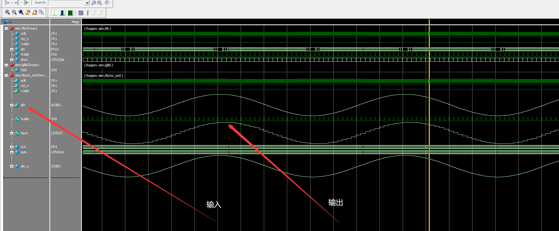
From the above we can see clearly that we have successfully achieved sinusoidal wave extraction. Thus the correctness of our experiment is verified.
CIC interpolation filter code
As for the code of CIC decimation filter, we use DDS to generate sine wave with sampling rate of 50MHz and frequency of 0.25MHz, and then reduce the sampling rate to 5MHz after 10 times decimation; after 10 times interpolation, finally verify its interpolation effect through 100 order CIC filter. The code is as follows:
CIC inter module:
`timescale 1ns / 1ps
// *********************************************************************************
// Project Name : OSXXXX
// Author       : zhangningning
// Email        : nnzhang1996@foxmail.com
// Website      :
// Module Name  : CIC_inter.v
// Create Time  : 2020-04-24 20:20:56
// Editor       : sublime text3, tab size (4)
// CopyRight(c) : All Rights Reserved
//
// *********************************************************************************
// Modification History:
// Date             By              Version                 Change Description
// -----------------------------------------------------------------------
// XXXX       zhangningning          1.0                        Original
//
// *********************************************************************************

module CIC_inter(
    //System Interfaces
    input                   sclk            ,
    input                   rst_n           ,
    //Communication Interfaces
    input                   rvalid          ,
    input           [12:0]  din             ,
    output  reg             tvalid          ,
    output  wire    [19:0]  dout
);

//========================================================================================\
//**************Define Parameter and  Internal Signals**********************************
//========================================================================================/
reg                 [ 9:0]  cnt             ;
wire                [19:0]  din_x           ;
wire                [19:0]  data            ;
reg                         data_valid      ;
reg                 [ 9:0]  cnt_cic         ;
reg                 [19:0]  sum             ;

//========================================================================================\
//**************     Main      Code        **********************************
//========================================================================================/
assign      din_x           =           {{7{din[12]}},din};
assign      data            =           din_x;
assign      dout            =           sum;

always @(posedge sclk or negedge rst_n)
    if(rst_n == 1'b0)
        cnt                 <=          10'd0;
    else if(cnt == 10'd0 && rvalid == 1'b1)
        cnt                 <=          cnt + 1'b1;
    else if(cnt > 0 && cnt == 'd9)
        cnt                 <=          10'd0;
    else if(cnt > 0)
        cnt                 <=          cnt + 1'b1;
    else
        cnt                 <=          10'd0;

always @(posedge sclk or negedge rst_n)
    if(rst_n == 1'b0)
        data_valid          <=          1'b0;
    else if(cnt == 10'd0 && rvalid == 1'b1)
        data_valid          <=          1'b1;
    else if(cnt > 0)
        data_valid          <=          1'b1;
    else
        data_valid          <=          1'b0;

always @(posedge sclk or negedge rst_n)
    if(rst_n == 1'b0)
        cnt_cic             <=          10'd0;
    else if(data_valid == 1'b1 && cnt_cic == 'd99)
        cnt_cic             <=          10'd0;
    else if(data_valid == 1'b1)
        cnt_cic             <=          cnt_cic + 1'b1;
    else
        cnt_cic             <=          cnt_cic;

always @(posedge sclk or negedge rst_n)
    if(rst_n == 1'b0)
        sum                 <=          16'd0;
    else if(data_valid == 1'b1 && cnt_cic == 'd99)
        sum                 <=          data;
    else if(data_valid == 1'b1)
        sum                 <=          sum + data;
    else
        sum                 <=          sum;

always @(posedge sclk or negedge rst_n)
    if(rst_n == 1'b0)
        tvalid              <=          1'b0;
    else if(data_valid == 1'b1)
        tvalid              <=          1'b1;
    else
        tvalid              <=          1'b0;

endmodule
cic module:
`timescale 1ns / 1ps
// *********************************************************************************
// Project Name : OSXXXX
// Author       : zhangningning
// Email        : nnzhang1996@foxmail.com
// Website      :
// Module Name  : cic.v
// Create Time  : 2020-04-24 15:08:16
// Editor       : sublime text3, tab size (4)
// CopyRight(c) : All Rights Reserved
//
// *********************************************************************************
// Modification History:
// Date             By              Version                 Change Description
// -----------------------------------------------------------------------
// XXXX       zhangningning          1.0                        Original
//
// *********************************************************************************

module cic(
    //System Interfaces
    input                   sclk            ,
    input                   rst_n           ,
    //Communication Interfaces
    input                   rvalid          ,
    input           [ 9:0]  din             ,
    output  reg             tvalid          ,
    output  reg     [12:0]  dout
);

//========================================================================================\
//**************Define Parameter and  Internal Signals**********************************
//========================================================================================/
reg                 [ 9:0]  cnt             ;
reg                 [12:0]  sum             ;
wire                [12:0]  din_x           ;


//========================================================================================\
//**************     Main      Code        **********************************
//========================================================================================/
assign  din_x           =       {{3{din[9]}},din};

always @(posedge sclk or negedge rst_n)
    if(rst_n == 1'b0)
        cnt             <=      10'd0;
    else if(rvalid == 1'b1 && cnt == 'd9)
        cnt             <=      10'd0;
    else if(rvalid == 1'b1)
        cnt             <=      cnt + 1'b1;
    else
        cnt             <=      cnt;

always @(posedge sclk or negedge rst_n)
    if(rst_n == 1'b0)
        sum             <=      13'd0;
    else if(rvalid == 1'b1 && cnt == 'd9)
        sum             <=      din_x;
    else if(rvalid == 1'b1)
        sum             <=      sum + din_x;
    else
        sum             <=      sum;

always @(posedge sclk or negedge rst_n)
    if(rst_n == 1'b0)
        dout            <=      13'd0;
    else if(rvalid == 1'b1 && cnt == 'd9)
        dout            <=      sum;
    else
        dout            <=      dout;

always @(posedge sclk or negedge rst_n)
    if(rst_n == 1'b0)
        tvalid          <=      1'b0;
    else if(rvalid == 1'b1 && cnt == 'd9)
        tvalid          <=      1'b1;
    else
        tvalid          <=      1'b0;

endmodule
CIC interpolation filter test code
tb module:
`timescale 1ns / 1ps
// *********************************************************************************
// Project Name : OSXXXX
// Author       : zhangningning
// Email        : nnzhang1996@foxmail.com
// Website      :
// Module Name  : tb.v
// Create Time  : 2020-04-24 16:00:12
// Editor       : sublime text3, tab size (4)
// CopyRight(c) : All Rights Reserved
//
// *********************************************************************************
// Modification History:
// Date             By              Version                 Change Description
// -----------------------------------------------------------------------
// XXXX       zhangningning          1.0                        Original
//
// *********************************************************************************

module tb();
reg                 sclk            ;
reg                 rst_n           ;
wire                rvalid          ;
wire        [ 7:0]  din             ;
wire                tvalid          ;
wire        [12:0]  dout            ;
wire        [15:0]  CIC_inter_data  ;
wire                CIC_inter_tvalid;

initial begin
    sclk            =           1'b0;
    rst_n           <=          1'b0;
    #(1000);
    rst_n           <=          1'b1;
end
always      #(10)       sclk        =           ~sclk;

dds_compiler_0 dds_compiler_0_inst (
  .aclk                         (sclk                       ),                              // input wire aclk
  .m_axis_data_tvalid           (rvalid                     ),  // output wire m_axis_data_tvalid
  .m_axis_data_tdata            (din                        )    // output wire [7 : 0] m_axis_data_tdata
);

cic cic_inst(
    //System Interfaces
    .sclk                       (sclk                       ),
    .rst_n                      (rst_n                      ),
    //Communication Interfaces
    .rvalid                     (rvalid                     ),
    .din                        ({{2{din[7]}},din}          ),
    .tvalid                     (tvalid                     ),
    .dout                       (dout                       )
);

CIC_inter CIC_inter_inst(
    //System Interfaces
    .sclk                       (sclk                       ),
    .rst_n                      (rst_n                      ),
    //Communication Interfaces
    .rvalid                     (tvalid                     ),
    .din                        (dout                       ),
    .tvalid                     (CIC_inter_tvalid           ),
    .dout                       (CIC_inter_data             )
);


endmodule
Simulation results of CIC interpolation filter
The project is simulated by Modelsim, and the results are as follows: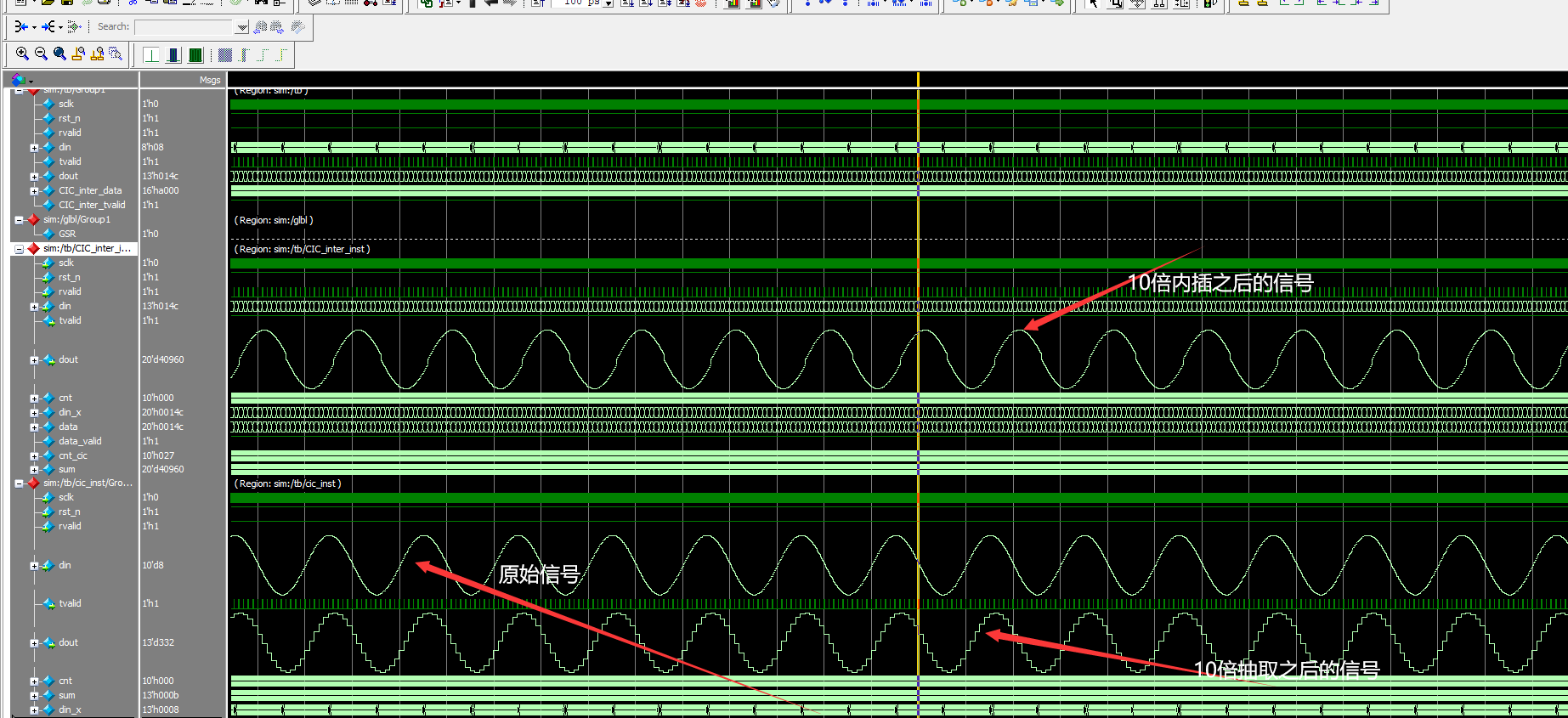
From the above results, it can be seen that the interpolation results are correct, but because the stopband attenuation of single-stage CIC filter is too low, so in practical engineering, multi-stage CIC filter is generally used for filtering, and the details will be discussed in our next blog.
reference
[1],FPGADesigner-CSDN Blogger
[2] , persistence of Longbow—— CSDN Blogger
[3] , statesmen—— CSDN Blogger
summary
When looking up some data, we found that some bloggers only gave part of the code, in fact, other people could not understand it at all, only giving the whole project code was easy to spread knowledge. It's not easy to create. Students who think the article is helpful can pay attention to it, like it and forward it. Contribute to the industry and a small part of it. Or students who have any opinions on the article or need to communicate further can join the following groups: