catalogue
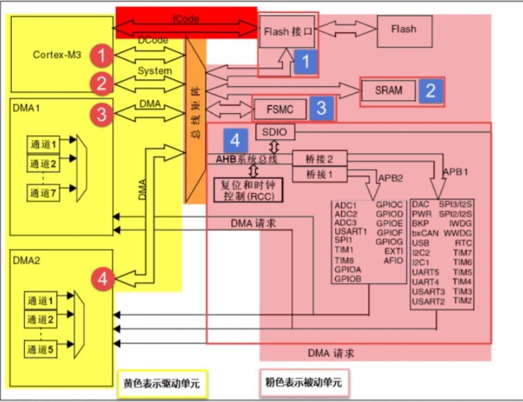
1. Address mapping and register mapping
2, Implementation of water lamp with C language register
3, Assembly language implementation of water lamp
1, Initialization
1. Address mapping and register mapping
Bus base address
| Bus name | Bus base address | Offset of external base address |
|---|---|---|
| APB1 | 0x4000 0000 | 0x0 |
| APB2 | 0x4001 0000 | 0x0001 0000 |
| AHB | 0x4001 8000 | 0x0001 8000 |
Peripheral base address
| Peripheral name | Peripheral base address | Address offset relative to APB2 bus |
|---|---|---|
| GPIOA | 0x4001 0800 | 0x0000 0800 |
| GPIOB | 0x4001 0C00 | 0x0000 0C00 |
| GPIOC | 0x4001 1000 | 0x0000 1000 |
| GPIOD | 0x4001 1400 | 0x0000 1400 |
| GPIOE | 0x4001 1800 | 0x0000 1800 |
| GPIOF | 0x4001 1C00 | 0x0000 1C00 |
| GPIOG | 0x4001 2000 | 0x0000 2000 |
Peripheral register address
Gpioa, gpiob and gpioc are used in this paper
| Register name | Register address | Offset from GPIOA base address |
|---|---|---|
| GPIOA_CRL | 0x4001 0800 | 0x00 |
| GPIOA_CRH | 0x4001 0804 | 0x04 |
| GPIOA_IDR | 0x4001 0808 | 0x08 |
| GPIOA_ODR | 0x4001 080C | 0x0C |
| GPIOA_BSRR | 0x4001 0810 | 0x10 |
| GPIOA_BRR | 0x4001 0814 | 0x14 |
| GPIOA_LCKR | 0x4001 0818 | 0x18 |
| Register name | Register address | Offset from GPIOB base address |
|---|---|---|
| GPIOB_CRL | 0x4001 0C00 | 0x00 |
| GPIOB_CRH | 0x4001 0C04 | 0x04 |
| GPIOB_IDR | 0x4001 0C08 | 0x08 |
| GPIOB_ODR | 0x4001 0C0C | 0x0C |
| GPIOB_BSRR | 0x4001 0C10 | 0x10 |
| GPIOB_BRR | 0x4001 0C14 | 0x14 |
| GPIOB_LCKR | 0x4001 0C18 | 0x18 |
| Register name | Register address | Offset from GPIOC base address |
|---|---|---|
| GPIOC_CRL | 0x4001 1000 | 0x00 |
| GPIOC_CRH | 0x4001 1004 | 0x04 |
| GPIOC_IDR | 0x4001 1008 | 0x08 |
| GPIOC_ODR | 0x4001 100C | 0x0C |
| GPIOC_BSRR | 0x4001 1010 | 0x10 |
| GPIOC_BRR | 0x4001 1014 | 0x14 |
| GPIOC_LCKR | 0x4001 1018 | 0x18 |
| Register name | Register address | Offset from GPIOD base address |
|---|---|---|
| GPIOD_CRL | 0x4001 1400 | 0x00 |
| GPIOD_CRH | 0x4001 1404 | 0x04 |
| GPIOD_IDR | 0x4001 1408 | 0x08 |
| GPIOD_ODR | 0x4001 140C | 0x0C |
| GPIOD_BSRR | 0x4001 1410 | 0x10 |
| GPIOD_BRR | 0x4001 0C14 | 0x14 |
| GPIOD_LCKR | 0x4001 0C18 | 0x18 |
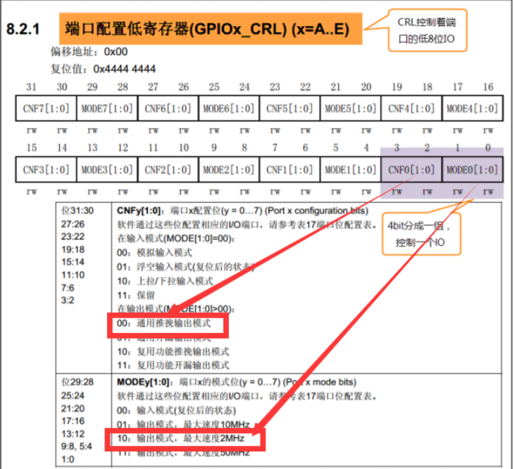
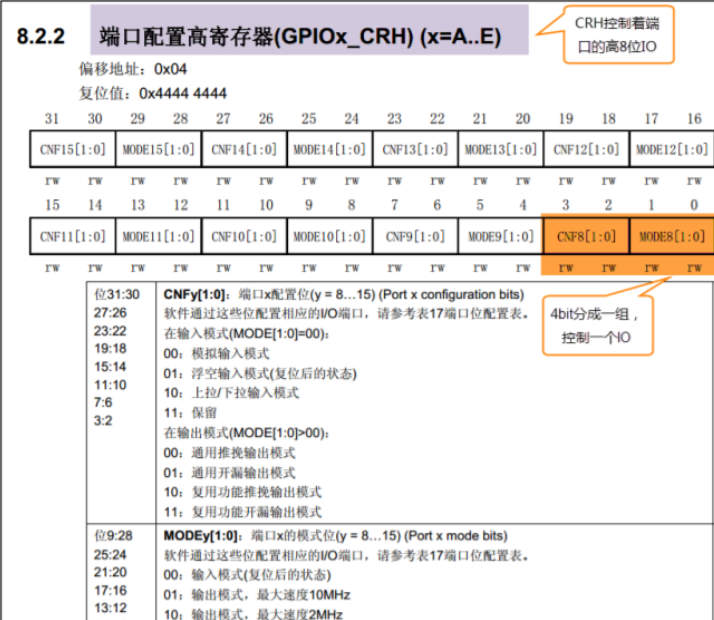
Because the stm32 smallest board has only three ABC pin series. Bits 0-7 are CRL and bits 8-15 are CRH. The offset relative to the base address is the number of hexadecimals from the base address. Different registers have different addresses. If you need to access the address, you need to look up the table.
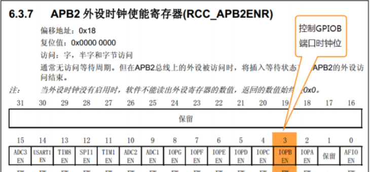
Clock register on APB2 line
Therefore, the subsequent codes are 0x00000002, corresponding to 0010
High order homology
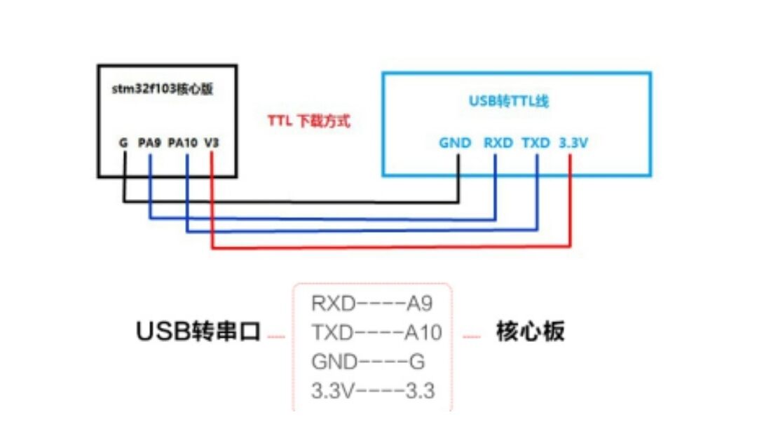
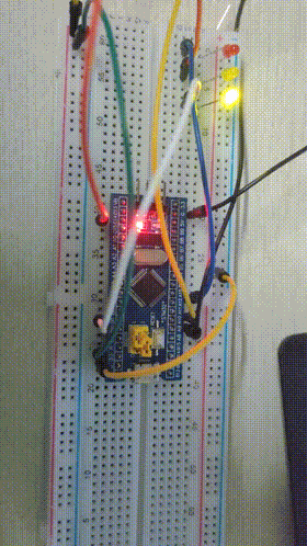
2. Wiring
Connect the serial port USB to TTL cable with the stm32 core board, as shown in the figure
And BOOT0 and BOOT1 should be set to configure the startup mode
| BOOT1=x | BOOT0=0 | Boot from user flash, this is the normal operating mode. |
| BOOT1=0 | BOOT0=1 | (ISP mode) start from the system memory. The program function started in this mode is set by the manufacturer. |
| BOOT1=1 | BOOT0=1 | Starting from the built - in SRAM, this mode can be used for debugging |
3. Program download
General wiring diagram
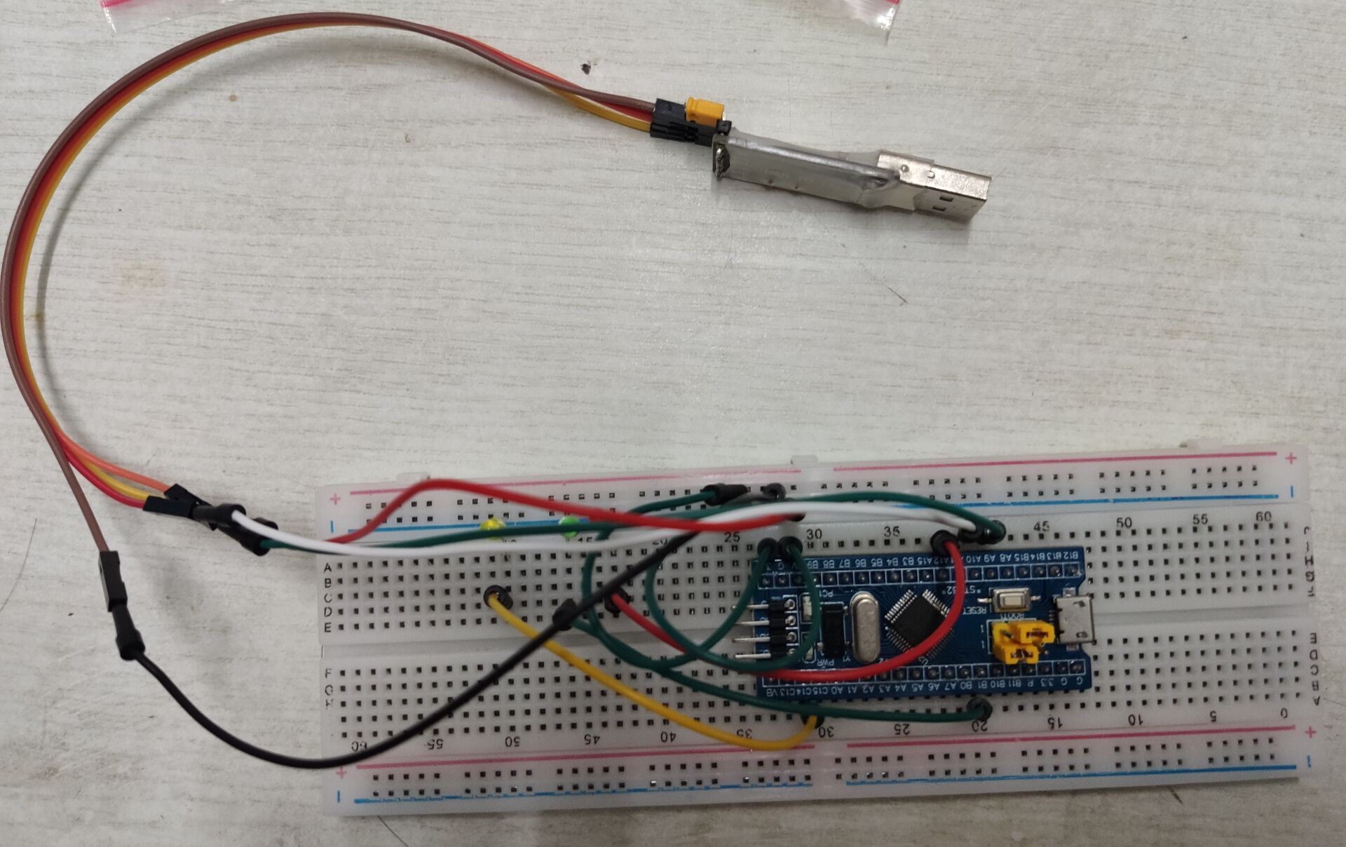
Because this paper mainly uses PA12, PB1 and pc14 pins.
2, Implementation of water lamp with C language register
Engineering documents
main.c
#define RCC_AP2ENR	*((unsigned volatile int*)0x40021018)
	//----------------GPIOA configuration register------------------------
#define GPIOA_CRH	*((unsigned volatile int*)0x40010804)
#define	GPIOA_ORD	*((unsigned volatile int*)0x4001080C)
//----------------GPIOB configuration register------------------------
#define GPIOB_CRL	*((unsigned volatile int*)0x40010C00)
#define	GPIOB_ORD	*((unsigned volatile int*)0x40010C0C)
//----------------GPIOC configuration register------------------------
#define GPIOC_CRH	*((unsigned volatile int*)0x40011004)
#define	GPIOC_ORD	*((unsigned volatile int*)0x4001100C)
//-------------------Simple delay function-----------------------
void  Delay_ms( volatile  unsigned  int  t)
{
     unsigned  int  i;
     while(t--)
         for (i=0;i<800;i++);
}
//------------------------Main function--------------------------
int main()
{
	int j=100;
	RCC_AP2ENR|=1<<2;			//APB2-GPIOA peripheral clock enable
	RCC_AP2ENR|=1<<3;			//APB2-GPIOB peripheral clock enable
	RCC_AP2ENR|=1<<4;			//APB2-GPIOC peripheral clock enable
	//These two lines of code can be combined into RCC_ APB2ENR|=1<<3|1<<4;
	GPIOA_CRH&=0xFFF0FFFF;		//Set bit reset
	GPIOA_CRH|=0x00020000;		//PA12 push pull output
	GPIOA_ORD|=1<<12;			//Set the initial light to on

	GPIOB_CRL&=0xFFFFFF0F;		//Set bit reset
	GPIOB_CRL|=0x00000020;		//PB1 push pull output
	GPIOB_ORD|=1<<1;			//Set the initial light to off

	GPIOC_CRH&=0xF0FFFFFF;		//Set bit reset
	GPIOC_CRH|=0x02000000;   	//PC14 push pull output
	GPIOC_ORD|=1<<14;			//Set the initial light to off
	while(j)
	{
		GPIOA_ORD=0x1<<12;		//PA12 high level
		Delay_ms(3000000);
		GPIOA_ORD=0x0<<12;		//PA12 low level
		Delay_ms(3000000);

		GPIOB_ORD=0x1<<1;		//PB1 high level
		Delay_ms(3000000);
		GPIOB_ORD=0x0<<1;		//PB1 low level
		Delay_ms(3000000);

		GPIOC_ORD=0x1<<14;		//PC14 high level
		Delay_ms(3000000);
		GPIOC_ORD=0x0<<14;		//PC14 low level
		Delay_ms(3000000);
	}
}
Use high level to turn on and low level to turn off
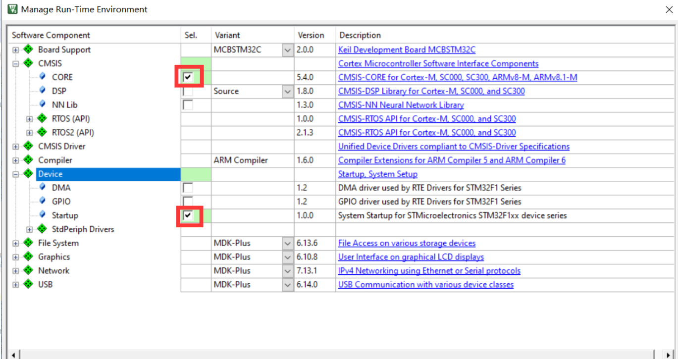
Add device
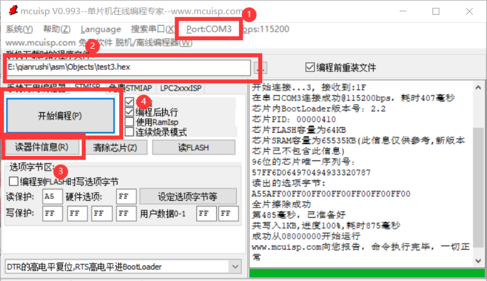
Compile the generated hex file and burn it into stm32 with mcuisp
Final results
3, Assembly language implementation of water lamp
Assembly code
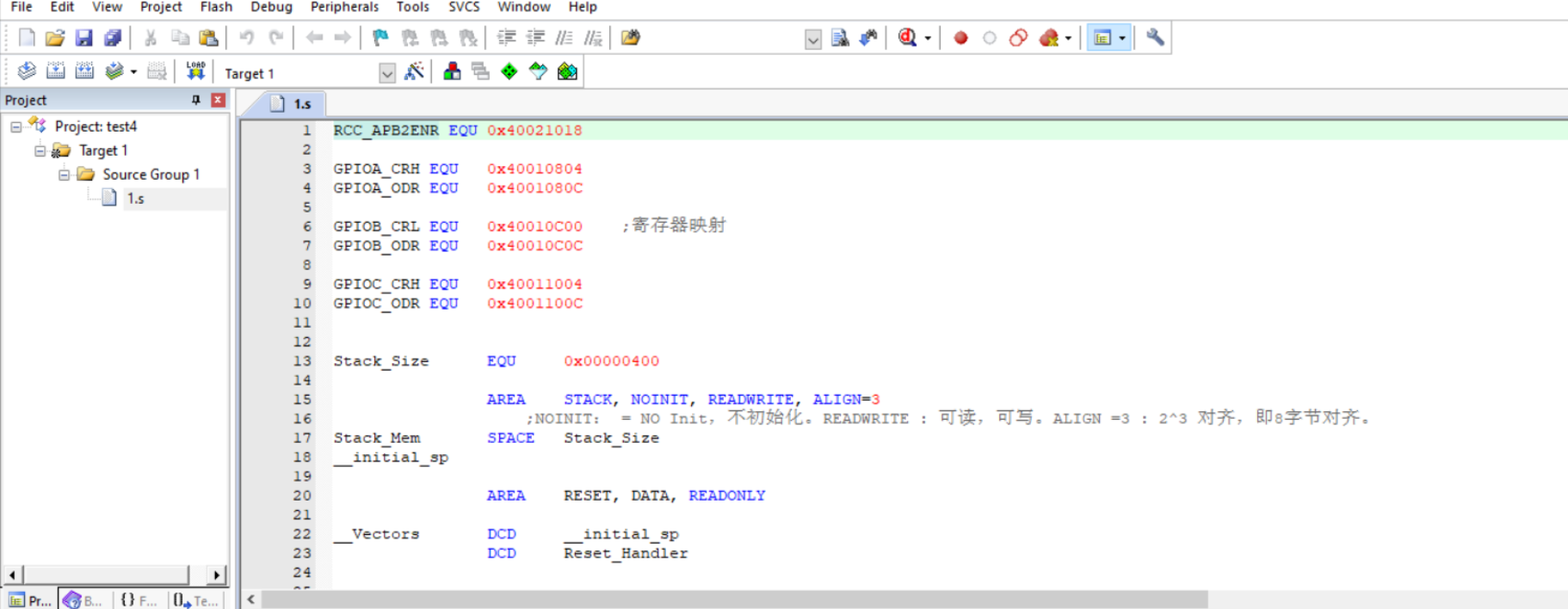
1.s
RCC_APB2ENR EQU 0x40021018
GPIOA_CRH EQU 0x40010804
GPIOA_ODR EQU 0x4001080C
GPIOB_CRL EQU 0x40010C00 ;Register mapping
GPIOB_ODR EQU 0x40010C0C
GPIOC_CRH EQU 0x40011004
GPIOC_ODR EQU 0x4001100C
Stack_Size EQU 0x00000400
AREA STACK, NOINIT, READWRITE, ALIGN=3
;NOINIT: = NO Init,Not initialized. READWRITE : Readable and writable. ALIGN =3 : 2^3 Alignment, i.e. 8-byte alignment.
Stack_Mem SPACE Stack_Size
__initial_sp
AREA RESET, DATA, READONLY
__Vectors DCD __initial_sp
DCD Reset_Handler
AREA |.text|, CODE, READONLY
THUMB
REQUIRE8
PRESERVE8
ENTRY
Reset_Handler
MainLoop BL LED2_Init
BL LED2_ON
BL Delay ;LED2 The lamp flashes
BL LED2_OFF
BL Delay
BL LED1_Init
BL LED1_ON
BL Delay ;LED1 The lamp flashes
BL LED1_OFF
BL Delay
BL LED3_Init
BL LED3_ON
BL Delay ;LED3 The lamp flashes
BL LED3_OFF
BL Delay
B MainLoop
LED1_Init
PUSH {R0,R1, LR} ;R0,R1,LR Put the values in the stack
LDR R0,=RCC_APB2ENR ;LDR Is to load the address into the register(such as R0).
ORR R0,R0,#0x08 ; Turn on the clock of port GPIOB, ORR operates by bit or, 01000 will set the second position of R0 to 1, and other bits remain unchanged
LDR R1,=RCC_APB2ENR
STR R0,[R1] ;STR Is to store the value in the address indicated by the register r0 The value stored in rcc register
;The above part of the assembly code controls the clock
LDR R0,=GPIOB_CRL
ORR R0,R0,#0X00000020 ;GPIOB_Pin_1 is configured as universal push-pull output; pb1 is turned on, so it is 2, 0010. It is a push-pull output mode, and the maximum speed is 2mhz
LDR R1,=GPIOB_CRL
STR R0,[R1]
LDR R0,=GPIOB_ODR
BIC R0,R0,#0X00000002 ;BIC reverses the immediate data first, and then compares it by bit
LDR R1,=GPIOB_ODR ;GPIO_Pin_1 The output is 0;from r1 control ord register
STR R0,[R1] ;take ord The value of the register becomes r0 Value of
POP {R0,R1,PC} ;Store the previously stored in the stack R0,R1,LR Value returned to R0,R1,PC
LED1_OFF
PUSH {R0,R1, LR}
LDR R0,=GPIOB_ODR
BIC R0,R0,#0X00000002 ; Because it is pb1, it corresponds to binary 0010;GPIO_Pin_1 output is 0, LED1 is off
LDR R1,=GPIOB_ODR
STR R0,[R1]
POP {R0,R1,PC}
LED1_ON
PUSH {R0,R1, LR}
LDR R0,=GPIOB_ODR
ORR R0,R0,#0X00000002 ;GPIO_Pin_1 output is 1, LED1 is on
LDR R1,=GPIOB_ODR
STR R0,[R1]
POP {R0,R1,PC}
LED2_Init
PUSH {R0,R1, LR};R0,R1,LR Put the values in the stack
LDR R0,=RCC_APB2ENR
ORR R0,R0,#0x04 ; Turn on the clock of GPIOA
LDR R1,=RCC_APB2ENR
STR R0,[R1]
LDR R0,=GPIOA_CRH
ORR R0,R0,#0X00020000 ;GPIOA_Pin_12 is configured as a universal push-pull output
LDR R1,=GPIOA_CRH
STR R0,[R1]
LDR R0,=GPIOA_ODR
BIC R0,R0,#0X00001000
LDR R1,=GPIOA_ODR ;GPIOA_Pin_12 The output is 0
STR R0,[R1]
POP {R0,R1,PC}
LED2_OFF
PUSH {R0,R1, LR}
LDR R0,=GPIOA_ODR
BIC R0,R0,#0X00001000 ;GPIOA_Pin_12 output is 0, LED2 is off
LDR R1,=GPIOA_ODR
STR R0,[R1]
POP {R0,R1,PC}
LED2_ON
PUSH {R0,R1, LR}
LDR R0,=GPIOA_ODR
ORR R0,R0,#0X00001000 ;GPIOA_Pin_12 output is 1, LED2 is on
LDR R1,=GPIOA_ODR
STR R0,[R1]
POP {R0,R1,PC}
LED3_Init
PUSH {R0,R1, LR}
LDR R0,=RCC_APB2ENR
ORR R0,R0,#0x10 ; Turn on the clock of GPIOC
LDR R1,=RCC_APB2ENR
STR R0,[R1]
LDR R0,=GPIOC_CRH
ORR R0,R0,#0X02000000 ;GPIOC_Pin_14 is configured as a universal push-pull output
LDR R1,=GPIOC_CRH
STR R0,[R1]
LDR R0,=GPIOC_ODR
BIC R0,R0,#0X00004000 ;GPIOC_Pin_14 output is 0
LDR R1,=GPIOC_ODR
STR R0,[R1]
POP {R0,R1,PC}
LED3_OFF
PUSH {R0,R1, LR}
LDR R0,=GPIOC_ODR
BIC R0,R0,#0X00004000 ;GPIOC_Pin_14 output is 0, LED3 goes out
LDR R1,=GPIOC_ODR
STR R0,[R1]
POP {R0,R1,PC}
LED3_ON
PUSH {R0,R1, LR}
LDR R0,=GPIOC_ODR
ORR R0,R0,#0X00004000 ;GPIOC_Pin_14 output is 1, LED3 is on
LDR R1,=GPIOC_ODR
STR R0,[R1]
POP {R0,R1,PC}
Delay
PUSH {R0,R1, LR}
MOVS R0,#0
MOVS R1,#0
MOVS R2,#0
DelayLoop0
ADDS R0,R0,#1
CMP R0,#300
BCC DelayLoop0
MOVS R0,#0
ADDS R1,R1,#1
CMP R1,#300
BCC DelayLoop0
MOVS R0,#0
MOVS R1,#0
ADDS R2,R2,#1
CMP R2,#15
BCC DelayLoop0
POP {R0,R1,PC}
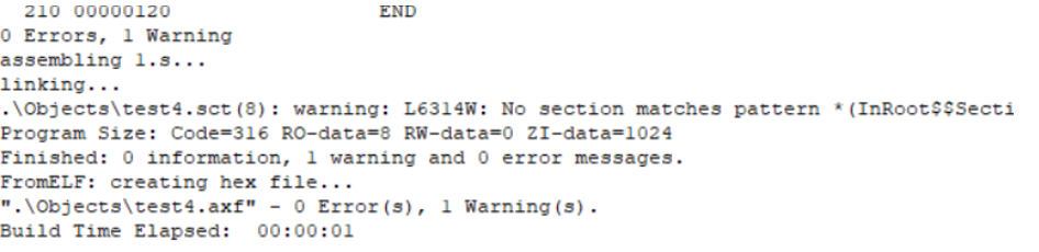
ENDAdd project file
Compile to generate hex file
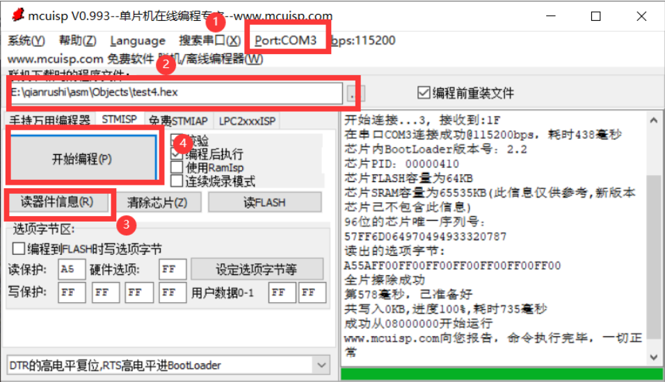
Burning program
Experimental results

4, Experience
I have a deep understanding of my own shortcomings in hands-on, but through consulting materials and consulting, I have slowly understood the working principle of stm32 and the conversion relationship of serial port, and really mastered the experiment of the combination of software and hardware. In fact, the operation of the whole experiment is cumbersome, and the experimental process and principle are very clear and easy to understand.
Reference connection: Based on assembly and C language, STM32 water lamp flashes in turn_ Laul Ken Yi's blog - CSDN blog