PWM - pulse width modulation
PWM module can generate PWM signal on GPIO. The module implements an up or down counter with four PWM channels to drive the allocated GPIO.
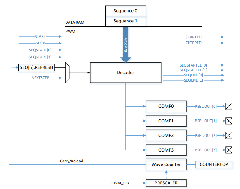
Three PWM modules can provide up to 12 PWM channels and up to 4 channels with a separate frequency control group. In addition, the built-in decoder and EasyDMA function can manipulate the PWM duty cycle without CPU intervention. Any duty cycle sequence can be read from the data RAM and can be linked to realize loop buffering or repeat into a complex loop.
Here are the main features of a PWM module:
- Fixed PWM fundamental frequency and programmable clock divider
- Up to four PWM channels with their respective polarity and duty cycle
- Pulse aligned along PWM channel or center
- Multiple duty cycle arrays (sequences) defined in Data RAM
- Automatic and fault free update of duty cycle directly from memory via EasyDMA
- Polarity, duty cycle and fundamental frequency may be changed at each PWM cycle
- The data RAM sequence can be repeated or connected to a loop
Wave counter
The wave counter is responsible for generating the duty cycle, which depends on the comparison value and the frequency depends on COUNTERTOP.
There is a common 15 bit counter with four comparison channels. Therefore, all four channels will share the same cycle (PWM frequency), but can have their own duty cycle and polarity. The polarity is set by the value read from RAM (see Figure 144: decoder memory access MODE on page 498), and the MODE register controls whether the counter counts up or up and down. The top value of the timer is controlled by the COUNTERTOP register. This register value is the same as PWM_ The selected PRESCALER combination of CLK will produce a given PWM cycle. A COUNTERTOP value less than the comparison setting will result in a state where no PWM edge is generated. Considering that the polarity is set to FallingEdge, set OUT[n] to a high value.
All comparison registers are internal and can only be configured through the decoder provided later.
The table can be written safely at any time. It will sample after the START task. If decoder. LOAD is not a waveform. It will also be sampled after the STARTSEQ[n] task and when a new value is loaded from RAM during sequence playback. If decoder. LOAD = waveform, the register value will be ignored and obtained from RAM (see decoder and easydma on page 498 below).
[nrf52] low_power_pwm pwm_library pwm_driver three differences
/********************************************************************************
* @file    bsp_pwm.c
* @author  jianqiang.xue
* @version V1.0.0
* @date    2021-08-10
* @brief   NULL
********************************************************************************/

/* Includes ------------------------------------------------------------------*/
#include "RTE_Components.h"
#include CMSIS_device_header
#include "nrf_drv_pwm.h"

#include "bsp_gpio.h"
#include "bsp_pwm.h"

/* Private includes ----------------------------------------------------------*/
#include "business_gpio.h"
#include "business_function.h"

/* Private variables ---------------------------------------------------------*/
static bool g_pwm_init = false;

#if BS_TIM1_EN
static nrf_drv_pwm_t m_pwm0 = NRF_DRV_PWM_INSTANCE(0);
static uint16_t const              m_pwm0_top   = BS_TIM1_PERIOD;
//static uint16_t const              m_pwm0_step  = 1;
static nrf_pwm_values_individual_t m_pwm0_seq_values;
static nrf_pwm_sequence_t const    m_pwm0_seq =
{
    .values.p_individual = &m_pwm0_seq_values,
    .length              = NRF_PWM_VALUES_LENGTH(m_pwm0_seq_values),
    .repeats             = 0,
    .end_delay           = 0
};
#endif

#if BS_TIM2_EN
static nrf_drv_pwm_t m_pwm1 = NRF_DRV_PWM_INSTANCE(1);
static uint16_t const              m_pwm1_top   = BS_TIM2_PERIOD;
//static uint16_t const              m_pwm1_step  = 1;
static nrf_pwm_values_individual_t m_pwm1_seq_values;
static nrf_pwm_sequence_t const    m_pwm1_seq =
{
    .values.p_individual = &m_pwm1_seq_values,
    .length              = NRF_PWM_VALUES_LENGTH(m_pwm1_seq_values),
    .repeats             = 0,
    .end_delay           = 0
};
#endif

#if BS_TIM3_EN
static nrf_drv_pwm_t m_pwm2 = NRF_DRV_PWM_INSTANCE(2);
static uint16_t const              m_pwm2_top   = BS_TIM3_PERIOD;
//static uint16_t const              m_pwm2_step  = 1;
static nrf_pwm_values_individual_t m_pwm2_seq_values;
static nrf_pwm_sequence_t const    m_pwm2_seq =
{
    .values.p_individual = &m_pwm2_seq_values,
    .length              = NRF_PWM_VALUES_LENGTH(m_pwm2_seq_values),
    .repeats             = 0,
    .end_delay           = 0
};
#endif

void bsp_pwm_init(void)
{
    if (g_pwm_init)
    {
        return;
    }
#if BS_TIM1_EN
    nrf_drv_pwm_config_t const config0 =
    {
        .output_pins =
        {
#if BS_TIM1_CH0_PIN != NULL
            BS_TIM1_CH0_PIN | NRF_DRV_PWM_PIN_INVERTED, // channel 0
#else
            NRF_DRV_PWM_PIN_NOT_USED,                   // channel 0
#endif
#if BS_TIM1_CH1_PIN != NULL
            BS_TIM1_CH1_PIN | NRF_DRV_PWM_PIN_INVERTED, // channel 1
#else
            NRF_DRV_PWM_PIN_NOT_USED,                   // channel 1
#endif
#if BS_TIM1_CH2_PIN != NULL
            BS_TIM1_CH2_PIN | NRF_DRV_PWM_PIN_INVERTED, // channel 2
#else
            NRF_DRV_PWM_PIN_NOT_USED,                   // channel 2
#endif
#if BS_TIM1_CH3_PIN != NULL
            BS_TIM1_CH3_PIN | NRF_DRV_PWM_PIN_INVERTED, // channel 3
#else
            NRF_DRV_PWM_PIN_NOT_USED,                   // channel 3
#endif
        },
        .irq_priority = APP_IRQ_PRIORITY_LOWEST,
        .base_clock   = (nrf_pwm_clk_t)BS_TIM1_PRESCALER,
        .count_mode   = NRF_PWM_MODE_UP,
        .top_value    = m_pwm0_top,
        .load_mode    = NRF_PWM_LOAD_INDIVIDUAL,
        .step_mode    = NRF_PWM_STEP_AUTO
    };
    APP_ERROR_CHECK(nrf_drv_pwm_init(&m_pwm0, &config0, NULL));

    m_pwm0_seq_values.channel_0 = 0x8000;
    m_pwm0_seq_values.channel_1 = 0x8000;
    m_pwm0_seq_values.channel_2 = 0x8000;
    m_pwm0_seq_values.channel_3 = 0x8000;

    (void)nrf_drv_pwm_simple_playback(&m_pwm0, &m_pwm0_seq, 1, NRF_DRV_PWM_FLAG_LOOP);
	g_pwm_init = true;
#endif

#if BS_TIM2_EN
    nrf_drv_pwm_config_t const config1 =
    {
        .output_pins =
        {
#if BS_TIM2_CH0_PIN != NULL
            BS_TIM2_CH0_PIN | NRF_DRV_PWM_PIN_INVERTED, // channel 0
#else
            NRF_DRV_PWM_PIN_NOT_USED,                   // channel 0
#endif
#if BS_TIM2_CH1_PIN != NULL
            BS_TIM2_CH1_PIN | NRF_DRV_PWM_PIN_INVERTED, // channel 1
#else
            NRF_DRV_PWM_PIN_NOT_USED,                   // channel 1
#endif
#if BS_TIM2_CH2_PIN != NULL
            BS_TIM2_CH2_PIN | NRF_DRV_PWM_PIN_INVERTED, // channel 2
#else
            NRF_DRV_PWM_PIN_NOT_USED,                   // channel 2
#endif
#if BS_TIM2_CH3_PIN != NULL
            BS_TIM2_CH3_PIN | NRF_DRV_PWM_PIN_INVERTED, // channel 3
#else
            NRF_DRV_PWM_PIN_NOT_USED,                   // channel 3
#endif
        },
        .irq_priority = APP_IRQ_PRIORITY_LOWEST,
        .base_clock   = (nrf_pwm_clk_t)BS_TIM2_PRESCALER,
        .count_mode   = NRF_PWM_MODE_UP,
        .top_value    = m_pwm1_top,
        .load_mode    = NRF_PWM_LOAD_INDIVIDUAL,
        .step_mode    = NRF_PWM_STEP_AUTO
    };
    APP_ERROR_CHECK(nrf_drv_pwm_init(&m_pwm1, &config1, NULL));

    m_pwm1_seq_values.channel_0 = 0x8000;
    m_pwm1_seq_values.channel_1 = 0x8000;
    m_pwm1_seq_values.channel_2 = 0x8000;
    m_pwm1_seq_values.channel_3 = 0x8000;

    (void)nrf_drv_pwm_simple_playback(&m_pwm1, &m_pwm1_seq, 1, NRF_DRV_PWM_FLAG_LOOP);
	g_pwm_init = true;
#endif

#if BS_TIM3_EN
    nrf_drv_pwm_config_t const config2 =
    {
        .output_pins =
        {
#if BS_TIM3_CH0_PIN != NULL
            BS_TIM3_CH0_PIN | NRF_DRV_PWM_PIN_INVERTED, // channel 0
#else
            NRF_DRV_PWM_PIN_NOT_USED,                   // channel 0
#endif
#if BS_TIM3_CH1_PIN != NULL
            BS_TIM3_CH1_PIN | NRF_DRV_PWM_PIN_INVERTED, // channel 1
#else
            NRF_DRV_PWM_PIN_NOT_USED,                   // channel 1
#endif
#if BS_TIM3_CH2_PIN != NULL
            BS_TIM3_CH2_PIN | NRF_DRV_PWM_PIN_INVERTED, // channel 2
#else
            NRF_DRV_PWM_PIN_NOT_USED,                   // channel 2
#endif
#if BS_TIM3_CH3_PIN != NULL
            BS_TIM3_CH3_PIN | NRF_DRV_PWM_PIN_INVERTED, // channel 3
#else
            NRF_DRV_PWM_PIN_NOT_USED,                   // channel 3
#endif
        },
        .irq_priority = APP_IRQ_PRIORITY_LOWEST,
        .base_clock   = (nrf_pwm_clk_t)BS_TIM3_PRESCALER,
        .count_mode   = NRF_PWM_MODE_UP,
        .top_value    = m_pwm1_top,
        .load_mode    = NRF_PWM_LOAD_INDIVIDUAL,
        .step_mode    = NRF_PWM_STEP_AUTO
    };
    APP_ERROR_CHECK(nrf_drv_pwm_init(&m_pwm2, &config2, NULL));

    m_pwm2_seq_values.channel_0 = 0x8000;
    m_pwm2_seq_values.channel_1 = 0x8000;
    m_pwm2_seq_values.channel_2 = 0x8000;
    m_pwm2_seq_values.channel_3 = 0x8000;

    (void)nrf_drv_pwm_simple_playback(&m_pwm2, &m_pwm2_seq, 1, NRF_DRV_PWM_FLAG_LOOP);
	g_pwm_init = true;
#endif
}

/**
 * @brief  PWN Function off
 * @note   NULL
 * @retval None
 */
void bsp_pwm_deinit(void)
{
    if (!g_pwm_init)
    {
        return;
    }
#if BS_TIM1_EN
	nrf_drv_pwm_uninit(&m_pwm0);
    g_pwm_init = false;
#endif
#if BS_TIM2_EN
	nrf_drv_pwm_uninit(&m_pwm1);
    g_pwm_init = false;
#endif
#if BS_TIM3_EN
	nrf_drv_pwm_uninit(&m_pwm2);
    g_pwm_init = false;
#endif
}

/**
 * @brief  Set PWM duty cycle
 * @note   NULL
 * @param  pwmx: PWM Group number
 * @param  val: 0-100 PWM value
 * @retval None
 */
void bsp_pwm_set_pulse(bsp_pwm_t pwmx, uint16_t val)
{
#if BS_TIM1_EN || BS_TIM2_EN
    if (!g_pwm_init)
    {
        return;
    }
#endif
    if (pwmx == BSP_PWM_0)
    {
#if BS_TIM1_EN && BS_PWM0_EN
        m_pwm0_seq_values.channel_0 = val;
#endif
    }
    else if (pwmx == BSP_PWM_1)
    {
#if BS_TIM1_EN && BS_PWM1_EN
        m_pwm0_seq_values.channel_1 = val;
#endif
    }
    else if (pwmx == BSP_PWM_2)
    {
#if BS_TIM1_EN && BS_PWM2_EN
        m_pwm0_seq_values.channel_2 = val;
#endif
    }
    else if (pwmx == BSP_PWM_3)
    {
#if BS_TIM1_EN && BS_PWM3_EN
        m_pwm0_seq_values.channel_3 = val;
#endif
    }
    else if (pwmx == BSP_PWM_4)
    {
#if BS_TIM2_EN && BS_PWM4_EN
        m_pwm1_seq_values.channel_0 = val;
#endif
    }
    else if (pwmx == BSP_PWM_5)
    {
#if BS_TIM2_EN && BS_PWM5_EN
        m_pwm1_seq_values.channel_1 = val;
#endif
    }
    else if (pwmx == BSP_PWM_6)
    {
#if BS_TIM2_EN && BS_PWM6_EN
        m_pwm1_seq_values.channel_2 = val;
#endif
    }
    else if (pwmx == BSP_PWM_7)
    {
#if BS_TIM2_EN && BS_PWM7_EN
        m_pwm1_seq_values.channel_3 = val;
#endif
    }
    else if (pwmx == BSP_PWM_8)
    {
#if BS_TIM3_EN && BS_PWM8_EN
        m_pwm2_seq_values.channel_0 = val;
#endif
    }
    else if (pwmx == BSP_PWM_9)
    {
#if BS_TIM3_EN && BS_PWM9_EN
        m_pwm2_seq_values.channel_1 = val;
#endif
    }
    else if (pwmx == BSP_PWM_10)
    {
#if BS_TIM3_EN && BS_PWM10_EN
        m_pwm2_seq_values.channel_2 = val;
#endif
    }
    else if (pwmx == BSP_PWM_11)
    {
#if BS_TIM3_EN && BS_PWM11_EN
        m_pwm2_seq_values.channel_3 = val;
#endif
    }
}
/********************************************************************************
* @file    bsp_pwm.h
* @author  jianqiang.xue
* @version V1.0.0
* @date    2021-04-18
* @brief   NULL
********************************************************************************/

#ifndef __BSP_PWM_H
#define __BSP_PWM_H

/* Includes ------------------------------------------------------------------*/
#include <stdint.h>

/* Public enum ---------------------------------------------------------------*/
typedef enum
{
    BSP_PWM_0 = 0,
    BSP_PWM_1,
    BSP_PWM_2,
    BSP_PWM_3,
    BSP_PWM_4,
    BSP_PWM_5,
    BSP_PWM_6,
    BSP_PWM_7,
    BSP_PWM_8,
    BSP_PWM_9,
    BSP_PWM_10,
    BSP_PWM_11
} bsp_pwm_t;

/* Public Function Prototypes ------------------------------------------------*/

void bsp_pwm_init(void);
void bsp_pwm_deinit(void);

void bsp_pwm_set_pulse(bsp_pwm_t pwmx, uint16_t val);

#endif