Blog introduction
This blog is the content of hardware description 3 of digital system experiment in my sophomore year. It is recorded here to prevent loss. The contents are as follows:
- Timing analysis of IIC serial bus
- VHDL programming design special state machine and two pieces of asynchronous FIFO to realize ping-pong operation
- Design HM62256 test circuit and verify it by simulation
- Custom development of a 1-port RAM IP core
Timing analysis of IIC serial bus
① Understand the timing of IIC bus reading arbitrary address data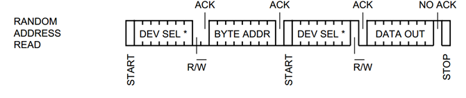
First, the SCL remains high, SDA drops down, and start. The host sends the 7-bit address code + Write direction "0" ("pseudo write") of the device, and releases the SDA line after sending and generates the 9th clock signal on the SCL line. After the selected device confirms its address, it generates the response signal on the SDA line. Then, the host sends another byte of the first address of the storage area of the device to be read out. After receiving the response, the host repeats the starting signal to send out the device address and reading direction ("1"). After receiving the response from the device, the data bytes can be read out. Every time a byte is read out, the host will reply to the response signal. When the last byte of data is read, the host returns to send a termination signal with "non acknowledge" (high level) to end the read-out operation
② Load the hex file into the MCU, start the simulation and master the read-write operation.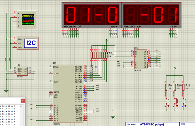
Read write operation:
The third button controls the address of 24C02C storage area, the second button controls the data to be written, and the first button presses to perform the write operation. The high two bits of the nixie tube represent the address of the 24C02C storage area, the fourth and fifth bits represent the input data, and the low two bits represent the data read out on the designated address of 24C02C. Therefore, you only need to control the key 3 to specify the address, the key 2 to specify the input data, and finally press the key 1 to store the data in the corresponding address; you only need to control the key 3 to specify the address, and then you can see the data output in the lower 2 bits of the nixie tube.
③ Refer to figure C for the data in IIC debugger, grab the corresponding waveform in the oscilloscope at this time, record and explain the operation process one by one.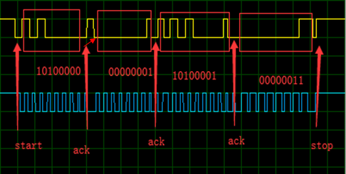
- Figure C is an arbitrary reading process, SDA is from high to low, start; first, SCM sends 7-bit address code 1010000 + pseudo-0 to form 8 bytes A0, which represents AT24C02C address.
- AT24C02C answers after confirming that it is its own address; then MCU receives the response and sends the address 01H of storage area
- In response to AT24C02C, the microcontroller repeats the starting signal once and sends out the device address and reading direction bit ("1") to get A1
- AT24C02C answers, takes out data 03H from 01H, and sends.
- The MCU sends out the termination signal to end the read-out operation stop.
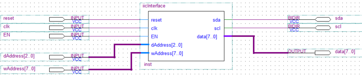
④ VHDL designs an interface circuit based on IIC bus to read any address data of 24C02C non-volatile memory and completes the simulation.
Design ideas: (the specific implementation is in the packaged engineering documents)
First of all, the timing division states for random reading are idle, sart, send memory address state, receive address state, read_data read status ack_for_read_data, response read state, stop state, etc.; for each state, it corresponds to the meaning of time sequence, and the entry of each state must meet the time sequence requirements. Then the input port has clk clock, reset, EN, and memory address signal ddaddress [2:0]; word address signal ddaddress [7:0]; for the address, these parallel data can be counted through a count variable count, and each time the count, a data bit can be transmitted to the sda.
- The implementation is as follows (the code still needs to be improved):
library ieee;
use ieee.std_logic_1164.all;
use ieee.std_logic_arith.all;
use ieee.std_logic_unsigned.all;
entity iicInterface is
port(
		reset,clk,EN:in std_logic;
		dAddress:in std_logic_vector(2 downto 0);
		wAddress:in std_logic_vector(7 downto 0);
		sda,scl:inout std_logic;
		data:out std_logic_vector(7 downto 0));
end iicInterface;
architecture Behavioral of iicInterface is
signal sdaTemp:std_logic:='1';
signal sclTemp:std_logic:='1';
signal dataTemp:std_logic_vector(7 downto 0):="00000000";
type state is (
				idle,                   		--Idle state
				start,                  		--start
				first_device_addr,       		--Memory address receiving status
				ack_for_first_device_addr,    	--Response memory address status
				word_addr,          			--Word address status
				ack_for_word_addr,      		--Response word address status
				second_device_addr,            	--Receive memory address status again
				ack_for_second_device_addr,    	--Response receive memory address status again
				read_data,             			--Read status
				ack_for_read_data,     			--Response read status
				stop);  						--Stop state
signal current_state:state;            			--current state

begin

sda<=sdaTemp;
scl<=sclTemp;

process(clk,reset)
variable count:integer range 0 to 40;
begin
if reset='0'then                        		--Idle state
	sdaTemp<='1';
	sclTemp<='1';
	current_state<=idle;
	count:=0;
elsif clk'event and clk='1' then        		--Rising edge of clock
	case current_state is               		--Start state
		when idle=>
			if(EN='1')then
				current_state<=start;
			else
				current_state<=idle;
			end if;

		when start=>							--Start state sdaTemp Pull to low level
			sdaTemp<='0';
			count:=0;
			current_state<=first_device_addr;

		when first_device_addr=>           		--Memory address receiving status
			count:=count+1;
			case count is
				when 1=>						--AT24C series EEPROM The fixed part of the chip is1010
					sdaTemp<='1';
					sclTemp<=not sclTemp;
				when 2=>
					sdaTemp<='0';
					sclTemp<=not sclTemp;
				when 3=>
					sdaTemp<='1';
					sclTemp<=not sclTemp;
				when 4=>
					sdaTemp<='0';
					sclTemp<=not sclTemp;
				when 5=>
					sdaTemp<=dAddress(2);
					sclTemp<=not sclTemp;
				when 6=>
					sdaTemp<=dAddress(1);
					sclTemp<=not sclTemp;
				when 7=>
					sdaTemp<=dAddress(0);
					sclTemp<=not sclTemp;
				when 8=>
					sdaTemp<='0';
					sclTemp<=not sclTemp;				--The reading and writing direction is0,Pseudograph
					current_state<=ack_for_first_device_addr;
					count:=0;
				when others=>					--Waiting for response
					sdaTemp<='Z';
					sclTemp<='Z';
					current_state<=ack_for_first_device_addr;
					count:=0;
				end case;

		when ack_for_first_device_addr=>		--Response memory address status
			sdaTemp<='Z';
			sclTemp<='Z';
			if sda='0' then
				sclTemp<=not sclTemp;
				current_state<=word_addr;
			end if;

		when word_addr=>                    	--Word address status
			count:=count+1;
			case count is
				when 1=>
					sdaTemp<=wAddress(7);
					sclTemp<=not sclTemp;
				when 2=>
					sdaTemp<=wAddress(6);
					sclTemp<=not sclTemp;
				when 3=>
					sdaTemp<=wAddress(5);
					sclTemp<=not sclTemp;
				when 4=>
					sdaTemp<=wAddress(4);
					sclTemp<=not sclTemp;
				when 5=>
					sdaTemp<=wAddress(3);
					sclTemp<=not sclTemp;
				when 6=>
					sdaTemp<=wAddress(2);
					sclTemp<=not sclTemp;
				when 7=>
					sdaTemp<=wAddress(1);
					sclTemp<=not sclTemp;
				when 8=>
					sdaTemp<=wAddress(0);
					sclTemp<=not sclTemp;
					current_state<=ack_for_word_addr;
					count:=0;
				when others=>
					sdaTemp<='Z';
					sclTemp<='Z';
					current_state<=ack_for_word_addr;
					count:=0;
			end case;

		when ack_for_word_addr=>				 --Response word address
		sdaTemp<='Z';
		sclTemp<='Z';
		if sda='0' then current_state<=second_device_addr;
			if sclTemp/='Z' then sclTemp<=not sclTemp;
			end if;
		end if;

		when second_device_addr=>           	--Receive memory address status again
			count:=count+1;
			case count is
				when 1=>						--AT24C series EEPROM The fixed part of the chip is1010
					sdaTemp<='1';
					sclTemp<=not sclTemp;
				when 2=>
					sdaTemp<='0';
					sclTemp<=not sclTemp;
				when 3=>
					sdaTemp<='1';
					sclTemp<=not sclTemp;
				when 4=>
					sdaTemp<='0';
					sclTemp<=not sclTemp;
				when 5=>
					sdaTemp<=dAddress(2);
					sclTemp<=not sclTemp;
				when 6=>
					sdaTemp<=dAddress(1);
					sclTemp<=not sclTemp;
				when 7=>
					sdaTemp<=dAddress(0);
					sclTemp<=not sclTemp;
				when 8=>
					sdaTemp<='1';					--The reading and writing direction is1
					sclTemp<=not sclTemp;
					current_state<=ack_for_second_device_addr;
					count:=0;
				when others=>
					sdaTemp<='Z';
					sclTemp<='Z';
					current_state<=ack_for_second_device_addr;
					count:=0;
				end case;

		when ack_for_second_device_addr=>		--Response receive memory address status again
			sdaTemp<='Z';
			sclTemp<='Z';
			if sda='0' then current_state<=read_data;
				if sclTemp/='Z' then sclTemp<=not sclTemp;
				end if;
			end if;
		when read_data=>
			count:=count+1;
			case count is
				when 1=>
					dataTemp(7)<=sda;
					sclTemp<=not sclTemp;
				when 2=>
					dataTemp(6)<=sda;
					sclTemp<=not sclTemp;
				when 3=>
					dataTemp(5)<=sda;
					sclTemp<=not sclTemp;
				when 4=>
					dataTemp(4)<=sda;
					sclTemp<=not sclTemp;
				when 5=>
					dataTemp(3)<=sda;
					sclTemp<=not sclTemp;
				when 6=>
					dataTemp(2)<=sda;
					sclTemp<=not sclTemp;
				when 7=>
					dataTemp(1)<=sda;
					sclTemp<=not sclTemp;
				when 8=>
					dataTemp(0)<=sda;
					sclTemp<=not sclTemp;
					data(7 downto 0)<=dataTemp(7 downto 0);
					current_state<=ack_for_read_data;
					count:=0;
				when others=>
					sdaTemp<='Z';
					sclTemp<='Z';
					current_state<=ack_for_read_data;
					count:=0;
		end case;
		when ack_for_read_data=>						--Response receive memory address status again
			if sda='1' then current_state<=stop;	--High level indicates termination
			else current_state<=read_data;
			sclTemp<=not sclTemp;
			end if;
		when stop=>
			current_state<=idle;
		when others=>						--Minimum risk
			current_state<=idle;
	end case;
end if;
end process;
end Behavioral;
- Top level:
- Simulation verification:
- Waveform analysis:
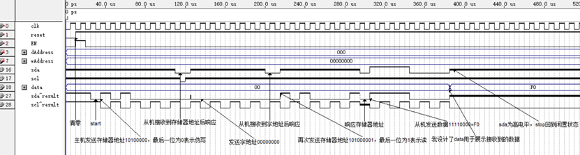
First set the reset, then EN effectively starts the random read sequence, sda is pulled down when sart, next the address of the memory file to be sent is 10100000, the number 000 is selected as 24C02C, and the last bit 0 indicates pseudo write; next 24C02C confirms that it is its own address sending response, sda is pulled down; next, the host receives the response, then sends the word address 00000000; 24C02C receives the word address, then sends the response; receives After the response, the host sends the memory address 10100001 again, the last bit 1 indicates reading; after the slave receives the response, it sends the data 11110000 with the word address 00000000; the host successfully reads the data F0. Finally, the host feedback sda as high level means that it will not read any more, and the slave will not send data at this time, and it will return to idle state, and sda and scl will be pulled high.
Conclusion: through verification, the interface circuit reads the data F0 of 24C02C address 00H, and displays it on the data side. The timing of the design circuit meets the requirements of random reading.
VHDL programming design special state machine and two pieces of asynchronous FIFO to realize ping-pong operation:
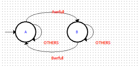
① The state machine is used to design the control module, including a and B States, which respectively represent the write in of FIFO A and FIFO B. the state machine input is the write full signal of two FIFOs, Awrfull and Bwrfull. When Awrfull is valid, it indicates that FIFO A is full and therefore changes from state a to state B. when Bwrfull is valid, it indicates that FIFO B is full and therefore changes from state B to state a.
② Output of state machine: the output includes Awrreq and Ardreq as write enable and read enable of FIFO A respectively. When it is in A state, awreq = 1, Ardreq=0 means to write A; when it is in B state, awreq = 0, Ardreq=1; it means to read A; in addition, for the enable signal of FIFO No. B, it can be obtained by reversing awreq and Ardreq.
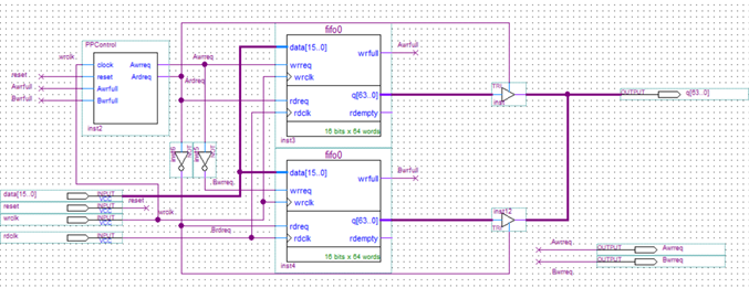
③ The state diagram and top-level implementation are shown in the figure below: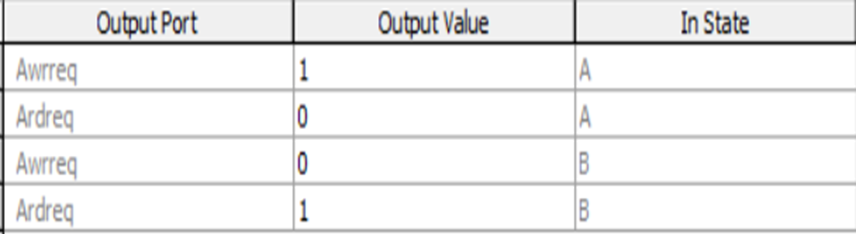
③ Simulation: set the write clock frequency of 40MHz and read clock frequency of 10MHz. In order to see the clock size relationship clearly, I changed the capacity of FIFO to 64, so it is only 64bit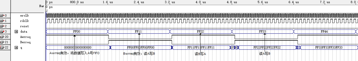
- Simulation analysis:
At 01.6us, Awrreq is valid, write A to read B, write FF00 to FIFO No. A, read data display 0000 because B is empty; 1.6us3.2us, Bwrreq is valid, write B to read A, write FF11 to FIFO No. B, read ff00FF00 in A; 3.2us~4.8us, Awrreq is valid, write A to read B, write FF22 to FIFO No. A, read ff11ff11ff11 in B The verification is completed by analogy and repetition.
Design HM62256 test circuit and verify it by simulation
- HM62256 test circuit is designed and verified by simulation.
(1) HM62256A is 32-kword × 8 static RAM, pin has address A0~14, chip selection CS low level is valid, WE write low level is valid, OE output low level is valid
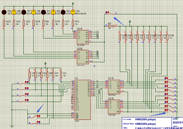
(2) New Proteus project, add devices, and design HM62256 function verification circuit:
(3) Simulation results show that HM62256 has the function of reading and writing, and the operation steps and experimental results are recorded.
① Write: first, set the address switch to A0A3=0000, the switch is fully closed, the data input switch to A7A0=10101010, and the switch is closed between phases; then set the WE to low level, the output signal OE to high level, and control the switch of the three state gate to close, and the write address is 0x0, and the data input is 10101010; you can see that the LED light group displays dark light, dark light, dark light, and dark light, indicating write Enter data 10101010.
② Read 0x0 address: next, set WE to low level in sequence, control signal switch of three state gate is on, and LED light is off. Finally, the output signal OE is set to low level. At the moment when the switch is closed, it can be seen that the LED is dark, dark, bright, dark and bright, indicating that the reading is successful.
③ Conclusion: the reading and writing operation is successful.
Custom development of a 1-port RAM IP core
(1) Customization steps: Tools → Mega wizard plug in manager → Create a new custom megafunction variation → installed plug ins → Memory Compiler → ram1 port → set the output q to 8 bits, with a total capacity of 32. The port RAM should be customized according to address 4 data 8, but the minimum capacity is 32, so only address 5 data 8 can be customized. Later, only 4-bit address is needed → create a new mif file, and set the 16 byte capacity. As shown in the figure below on the left: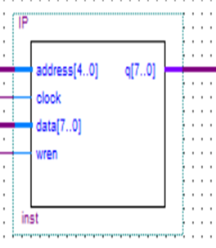
(2) Analyze and explain how to generate html waveform report in the directory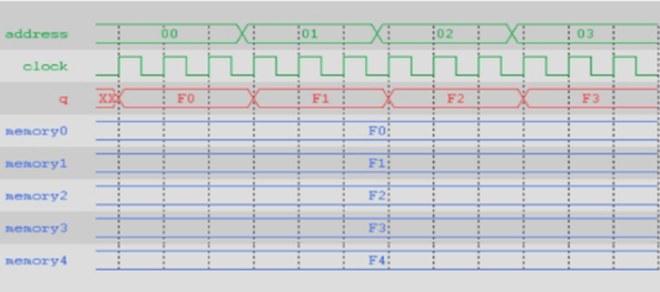
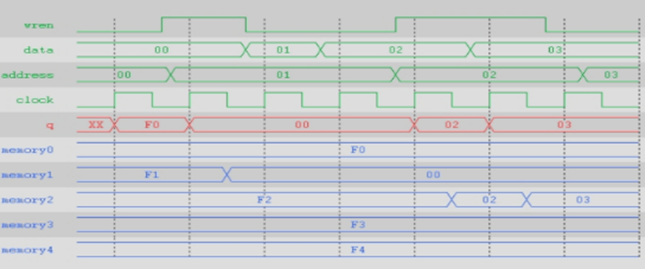
① Figure 1 is the waveform of the read operation. The read occurs at the rising edge of the clock cycle when the enable is 0. Read the value F0 of address 00 on the rising edge of 13 clock, and read the value F1 of address 01 on the rising edge of 45 clock. Similarly, read F2 and F3 respectively on the rising edge of subsequent clock.
② Figure 2 is the waveform of write operation. When wren is high enabled and at the rising edge of the clock, the input is loaded to the output end, and only at the falling edge of this cycle can the RAM be truly written. The data input is loaded into the output at the rising edge of the second clock cycle, and the memory0 is written at the falling edge. Similarly, the input 02 and 03 are written into memory2 at the falling edge of the fifth and sixth clock cycles respectively
(3) The function of reading and writing is verified by simulation, and the oscillogram is recorded and explained.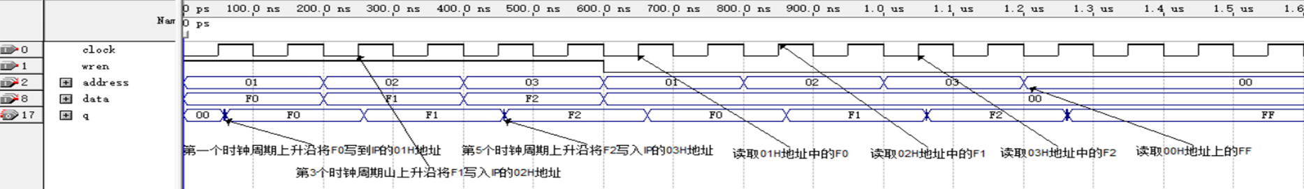
Analysis: set wren to high level for 0~600ns, and perform write operation. The rising edge of the first clock writes F0 to the 01H address of the IP, the rising edge of the second clock writes F1 to the 02H address of the IP, and the rising edge of the fifth clock writes F2 to the 02H address of the IP; after 600ns, set wren signal to low level, perform the read operation, and perform the read operation at the rising edge of 650ns, 850ns, 1050ns, respectively, reading F0, F1, F2 of the 01H, 02H, 03H addresses.
Conclusion: the data written in address 01H, 02H, 03H is consistent with the data read, and the IP read-write function is verified correctly.