1. Parallel port is often used for FPGA and cpu chip communication, configuration register, cross chip data transmission, etc
2. Source synchronous transmission: the sender sends the clock and data to the receiver at the same time, and the receiver uses the clock sampling data sent by the source.
3. Asynchronous parallel port communication:
Asynchronous parallel port application:
--cpu chips (dsp, stm32) interact with FPGA data. The data rate is generally within 100Mbps, and the data bus is no more than 16bit
--Non cpu functional chips interact with FPGA through parallel port, such as configuration register, etc
Parallel port signal description:
--Chip select chip select signal, abbreviated as cs_n, which is low effective. When it is pulled low, it means that the parallel port of the device is activated.
--Write enable write enable signal, which is abbreviated as "we",, the signal is low and effective. When you do not pull down, it means that the address data of the address bus and data bus is written.
--Read enable read enable signal, abbreviated as Rd ﹣ n, which is low and effective. When not pulled down, it means that the address and data of address bus and data bus are
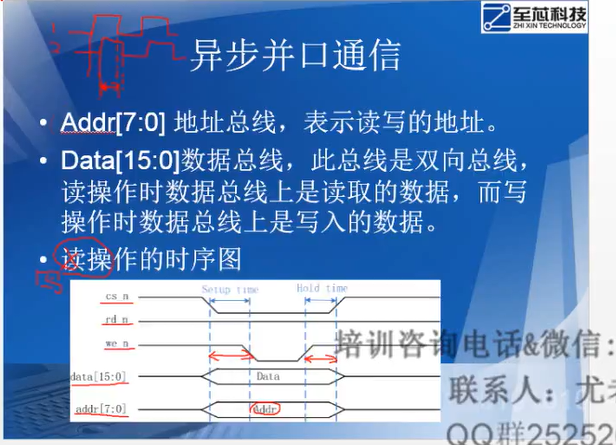
--Addr[7:0] address bus, which represents the read-write address.
--Data[15:0] data bus, which is a two-way bus. During the read operation, the data is read on the data bus, while during the write operation, the data is written on the data bus.
--Write operation sequence is shown in Figure
--Parallel port is not suitable for high-speed transmission and occupies a lot of pins. Its advantages are simple and logic simple
--Read operation sequence is shown in Figure

--Read wait (set to 40ns) is assigned to the port after the address data is stable.
4. Store data in register and address register
5. CS and WR are signals of two handshake operations
6. Register beat delay -- the number of delay clocks is n, and the data to be delayed is xbit. The format of delay using shift register is:
reg [3*n,0] Data_r;
Data [u r < = {data [u r [(n-1) * x, 0], data}; -- the high n-bit of data [u r] after the last three clocks is the output after delay.
For example:
Data_r < = {data_r [31:0], data}; / / data is 16bit, three beats are needed, so the total beat register is 16*3=48bit, and the previous one is 16*2=32bit
Addr ﹐ r < = {addr ﹐ R [15:0], addr}; / / addr is 8 bit, three beats are needed, so the total beat register is 8 * 3 = 14 bit, and the previous one is 8 * 2 = 16 bit
7. When the task contains parameters, the parameters need to be declared in the task
task write_data(len); //len needs to be declared below
 integer i, len;
 begin
  for(i=0; i
  begin
   ...
  end
  cs_n = 1;
 end
endtask
8. Use and test of tristate gate:
--Three state gate of source program module
reg    [2:0] cs_n_r, rd_n_r, wr_n_r;
inout tri  [15:0] data; //Two way port data line
assign data = (cs_n_r[2] == 1'b0 && rd_n_r[2] == 1'b0) ? rdata : 16'hzzzz;
--Three state gate of test module
reg      wr_n;
tri    [15:0] w_data;
assign w_data = (wr_n == 1'b0) ? data_tb : 16'hzzzz;

parall_interf parall_interf_inst( //Instantiation
 .sclk (sclk ),
 .rst_n (rst_n ),
 .cs_n (cs_n ),
 .rd_n (rd_n ), //Reading enable
 .wr_n (wr_n ), //Write enable
 .addr (addr ), //Address bus

 .data  (w_data )//Two way port data line -- when two-way port w'u data is output, data is input; on the contrary, when w'u data is input, data is input
);
9. Source file design code (parallel_inter. V)
module		parall_interf(
		input				wire				sclk,  //50Mhz
		input				wire				rst_n,
		input				wire				cs_n,
		input				wire				rd_n,//Reading enable
		input				wire				wr_n,//Write enable
		inout				tri					[15:0]		data,  //1Mhz two-way port data line
		input				wire				[7:0]			addr  //Address bus

);

//reg [15:0] data buf [7:0]; / / declare 8 16 bit registers
reg			[15:0]		data_0,data_1,data_2,data_3,data_4,data_5,data_6,data_7;
reg			[2:0]			cs_n_r,rd_n_r,wr_n_r;
reg			[47:0]		data_r;
reg			[23:0]		addr_r;
reg			[15:0]		rdata;


//Reduce the probability of metastability, and beat the CS, RD, and WR single bit signals twice
always @(posedge	sclk or negedge rst_n)
			if(rst_n==1'b0)
					{cs_n_r,rd_n_r,wr_n_r}<=9'h1ff;
			else
					{cs_n_r,rd_n_r,wr_n_r}<={{cs_n_r[1:0],cs_n},{rd_n_r[1:0],rd_n},{wr_n_r[1:0],wr_n}};

//Data is delayed to synchronize with the enable signal
always @(posedge	sclk or negedge rst_n)
			if(rst_n ==1'b0)
					begin
							data_r<=48'd0;
							addr_r<=24'd0;
					end
			else
					begin
							data_r<={data_r[31:0],data}; //The first shot: {data ﹣ R [31:0], data ﹣ 1} the second shot {data ﹣ R [15:0], data ﹣ 1, data ﹣ 2}
							//Three beats, the total beat register is 16*3=48bit, the front is 16*2=32bit
							//data_r[47:32]<=data_r[31:16];
							//data_r[31:16]<=data_r[15:0];
							//data_r[15:0]<=data;
							addr_r<={addr_r[15:0],addr};
					end

//Write operation, store the data on the data line into the corresponding register
always @(posedge sclk or negedge rst_n)
			if(rst_n==1'b0)
					begin
				  		data_0<=8'd0;
				  		data_1<=8'd0;
				  		data_2<=8'd0;
				  		data_3<=8'd0;
				  		data_4<=8'd0;
				  		data_5<=8'd0;
				  		data_6<=8'd0;
				  		data_7<=8'd0;
				  end
			 else if(cs_n_r[2]==1'b0 && rd_n_r[2] == 1'b1 && wr_n_r[2] ==	1'b0)
					case(addr_r[23:16])
							8'd0:data_0<=data_r[47:32];
							8'd1:data_1<=data_r[47:32];
							8'd2:data_2<=data_r[47:32];
							8'd3:data_3<=data_r[47:32];
							8'd4:data_4<=data_r[47:32];
							8'd5:data_5<=data_r[47:32];
							8'd6:data_6<=data_r[47:32];
							8'd7:data_7<=data_r[47:32];
				  default:
				  		begin
				      		data_0<=data_0;
				      		data_1<=data_1;
				      		data_2<=data_2;
				      		data_3<=data_3;
				      		data_4<=data_4;
				      		data_5<=data_5;
				      		data_6<=data_6;
				      		data_7<=data_7;
				     	end
				  endcase


always @(posedge sclk or negedge rst_n)
			if(rst_n == 1'b0)
					rdata <= 'd0;
			else if(cs_n_r[2]==1'b0 &&  wr_n_r[2] ==	1'b1)
					case(addr_r[23:16])
							8'd0:rdata<=data_0;
							8'd1:rdata<=data_1;
							8'd2:rdata<=data_2;
							8'd3:rdata<=data_3;
							8'd4:rdata<=data_4;
							8'd5:rdata<=data_5;
							8'd6:rdata<=data_6;
							8'd7:rdata<=data_7;
					    default:rdata <= 16'd0;
				  endcase

//Tristate gate -- when rd_n is low, assign rdata to data
assign data =(cs_n_r[2] ==1'b0 && rd_n_r[2]==1'b0)?rdata:16'hzzzz;

endmodule
10. Code in simulation sim (tb_parallel_inter. V)
`timescale  1ns/1ns
module 	tb_parall_interf();

parameter		setup_time = 2;  //Establish events
parameter		hold_time	=	2;	 //Retention time
parameter		data_time = 4;   //Duration
parameter		read_wait = 5;   //Read data waiting delay

reg					sclk,rst_n;
reg					cs_n,rd_n,wr_n;   //Enable
reg		[15:0]		data_tb;//Writing data
reg		[7:0]	    addr;
tri		[15:0]		w_data;//The output of inout terminal can only be connected to wire variable or tri variable

always  #10 sclk = ~sclk;

//Three state gate of test excitation
assign  w_data = (wr_n == 1'b0)?data_tb:16'hzzzz;

initial
				begin
							sclk = 0;
							rst_n = 0;
							#200;
							rst_n = 1;
				end

//Call task and initialize
initial
		begin
				cs_n=1;
				rd_n=1;
				wr_n=1;
				data_tb=0;
				addr=0;
				@(posedge	rst_n);
				#100;
				write_data(8);
				#100;
				read_data(8);
		end

//integer		i,len;
//Write data task, simulate cpu sending data to fpga, and nested tasks in task
integer		i,len;
task		write_data(len);
				integer		i;
				begin
						for(i=0;i<len;i=i+1)
						begin
								 //@ (posedge sclk);
								cs_n=0;
								data_tb=i[15:0];//Write operation: cpu writes address + data to fpga
								addr=i[7:0];
								setup_dly();
								wr_n=0;
								data_dly();
								wr_n=1;
								hold_dly();
						end
						cs_n=1; //When the cpu continuously writes data to the FPGA, CS ﹣ n can not be pulled up, and then it can be pulled up after all data has been written
				end
endtask

//Read data analog fpga read cpu
task		read_data(len);
				integer		i;
				begin
						for(i=0;i<len;i=i+1)
						begin
								cs_n=0;
								addr=i[7:0];
								read_dly();
								rd_n=0;
								data_dly();
								$display("read data addr is %d = %d",i,w_data);
								rd_n=1;
						end
						cs_n=1;
				end
endtask

parall_interf 	parall_interf_en(
		.sclk       (sclk ),
		.rst_n      (rst_n),
		.cs_n       (cs_n ),
		.rd_n       (rd_n ), //Reading enable
		.wr_n       (wr_n ),//Write enable
		.data       (w_data ),  //Two way port data line, when two-way port w_data is output, data is input; on the contrary.
		.addr       (addr ) //Address bus

);

//Basic delay tasks
task		setup_dly();
		integer  i;
		begin
				for(i=0;i<setup_time;i=i+1)
				begin
						@(posedge	sclk);
				end
		end
endtask

task		hold_dly();
		integer  i;
		begin
				for(i=0;i<hold_time;i=i+1)
				begin
						@(posedge	sclk);
				end
		end
endtask

task		data_dly();
		integer  i;
		begin
				for(i=0;i<data_time;i=i+1)
				begin
						@(posedge		sclk);
				end
		end
endtask

task		read_dly();
		integer  i;
		begin
				for(i=0;i<read_wait;i=i+1)
				begin
						@(posedge		sclk);
				end
		end
endtask
endmodule
11. Create the simulation script run.do file
quit -sim
.main clear

vlib	work
vmap	work work

vlog  ./tb_parall_interf.v
vlog  ./../design/parall_interf.v

vsim	-voptargs=+acc work.tb_parall_interf

add  wave  tb_parall_interf/*

add  wave  tb_parall_interf/parall_interf_en/*


run 10us
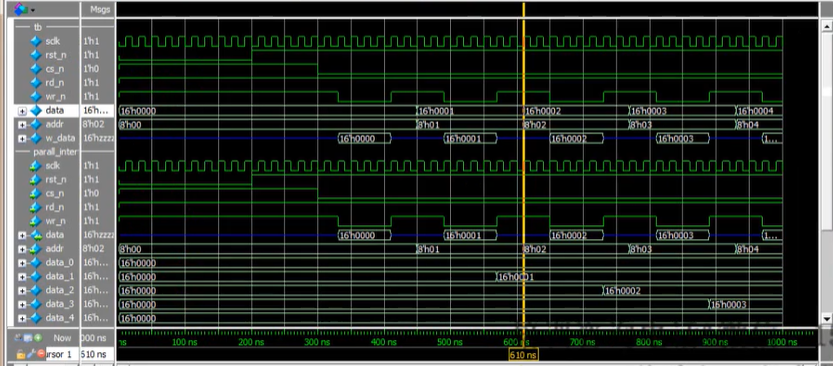
12. Simulation results