I've done this part of work before, but I haven't sorted it out. Now let's review it.
When the FPGA version comes out, how to make the AD9361 move is the top priority. At that time, I was very concerned about whether SPI passed?
- ENSM
The AD9361 transceiver includes an enable state machine (ENSM) that allows real-time control of the current state of the device. During normal operation, the device can be placed in a variety of different states, including
• Standby - energy saving, frequency synthesizer disabled
• Sleep - standby, all clocks / BB PLL s are disabled
• TX - TX signal chain enabled
• RX - RX signal chain enabled
• FDD-TX and RX signal chains are enabled
• Alarm - frequency synthesizer enabled

The gray state in the figure above does not need user control, and enters the next state after the set time. TO_ The ALERT bit is in the ENSM configuration register. If you want to switch to the WAIT state, you need to clear to in the RX or TX state_ ALERT bit, so that when moving out of Rx, Tx or FDD state, ENSM will transfer to WAIT state if to_ When ALERT is set to 1, ENSM will transition to ALERT state.
ENSM has two possible control methods: SPI control and pin control.
1) The ENSM can be controlled asynchronously by pushing the current state to the next state through SPI write register.
2) Use ENABLE and TXNRX pins to control the current state in real time
2.SPI control
In SPI control mode, write SPI register to enter the next state from the current state, so as to realize asynchronous control of ENSM. SPI control is considered to be related to DATA_CLK is asynchronous because SPI_CLK may derive from a different reference clock and still work. When it is not necessary to control the frequency synthesizer in real time, SPI control ENSM method is recommended. SPI control can be used for real-time control as long as the BBIC can accurately perform SPI write operations.
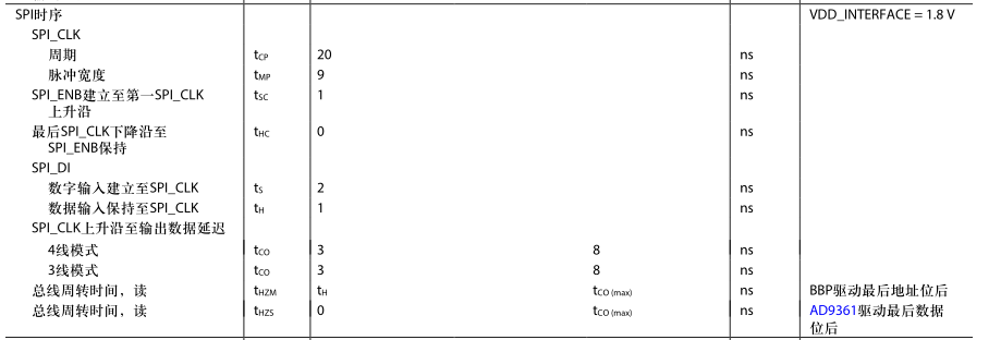
SPI interface
The AD9361 communicates with the BBP through a serial peripheral interface (SPI). The interface can be configured as a 4-wire interface with special receiving and transmitting ports, or as a 3-wire interface with a two-way data communication port. The bus allows BBP to set all device control parameters through a simple address data serial bus protocol.
Write command
Follow a 24 bit format. The first 6 bits are used to set the bus direction and the number of bytes to be transmitted. Write address of the next 10 bit data. The last 8 bits are the data to be transferred to the specified register address (MSB to LSB). AD9361 also supports LSB priority format, allowing commands to be written in LSB to MSB format. In this mode, for multi byte write commands, the register address will be incremented.
/**
 * SPI register write.
 * @param spi
 * @param reg The register address.
 * @param val The value of the register.
 * @return 0 in case of success, negative error code otherwise.
 */
int32_t ad9361_spi_write(struct spi_device *spi, uint32_t reg, uint32_t val)
{
	uint8_t buf[3];
	int32_t ret;
	uint16_t cmd;
	//uart_printf("ad9361_spi_write:reg[%d] = 0x%x\r\n",reg,val);
	cmd = AD_WRITE | AD_CNT(1) | AD_ADDR(reg);
	buf[0] = cmd >> 8;
	buf[1] = cmd & 0xFF;
	buf[2] = val;

	ret = spi_write_then_read(spi, buf, 3, NULL, 0);
	if (ret < 0) {
		dev_err(&spi->dev, "Write Error %"PRId32, ret);
		return ret;
	}
	return 0;
}
Read command
Follow a similar format, except that the first 16 bits are in SPI_ Transmitted on di pin, the last 8 bits are read from AD9361. If it is in 4-wire mode, it is in SPI_ Done on the do pin. If it is in 3-wire mode, it is in SPI_ Complete on di pin.
/**
 * SPI multiple bytes register read.
 * @param spi
 * @param reg The register address.
 * @param rbuf The data buffer.
 * @param num The number of bytes to read.
 * @return 0 in case of success, negative error code otherwise.
 */
int32_t ad9361_spi_readm(struct spi_device *spi, uint32_t reg,
	uint8_t *rbuf, uint32_t num)
{
	uint8_t buf[2];
	int32_t ret;
	uint16_t cmd;

	if (num > MAX_MBYTE_SPI)
		return -EINVAL;

	cmd = AD_READ | AD_CNT(num) | AD_ADDR(reg);
	buf[0] = cmd >> 8;
	buf[1] = cmd & 0xFF;

	ret = spi_write_then_read(spi, &buf[0], 2, rbuf, num);
	if (ret < 0) {
		dev_err(&spi->dev, "Read Error %"PRId32, ret);
		return ret;
	}
	return 0;
}
SPI timing